


1. Introduction
The development of nanomaterials technology directly drives the progress of scientific technology, which is facilitated by the development of technology and new instruments. Two-dimensional materials have gained significant attention in the scientific field due to their unique properties and potential applications in electronics, energy and other fields [1]. However, characterizing these materials at the nanoscale is still a challenging task. Scanning electron microscopy is a powerful imaging technique that enables high distinguishability imaging and analysis of materials' surface morphology, structure and composition. The morphology and composition of nanomaterials play a decisive role in the overall properties of materials, while SEM has tremendous advantages in investigating the microscopic morphology of materials and is indispensable, especially in materials analysis and preparation. In recent years, scanning electron microscopy has been widely used to study the properties of two-dimensional materials, providing a foundation for studying their structural properties, electronic behavior and other properties [2]. In this paper, the structure, working principle and characteristics of scanning electron microscope are first introduced, followed by the introduction of two-dimensional materials, including their definition, properties, preparation and applications, then SEM is introduced to characterize two-dimensional materials, and different examples show the advantages of SEM in characterization techniques. Finally, there is a summary of the whole paper and an outlook for future technique development.
2. Scanning electron microscope
2.1. General introduction of SEM
Scanning electron microscopy has irreplaceable advantages in the analysis and characterization of surface micro-morphology. Therefore, it is widely used in the development and research process of materials science. In 1965, the first commercial scanning electron microscope was brought to the market by the instrument company headed by Charles Otley's team, which marked the rapid development stage of SEM, about the principle of operation of scanning electron microscope [3]. SEM emits electrons mainly through an electron gun, which forms a high-energy electron beam after an accelerating electric field, and scans the sample in a regular sequence under the magnetic field of the scanning galvanic ring, then records the image information using a detector. The high-speed electrons' rapid interactions with the material's atoms result in a variety of electrical signals. An image is created by fusing the position of the electron beam with the strength of the signal being detected, and this image can then be presented on the screen using an image processing device [3]. Figure 1 below shows how an SEM works.
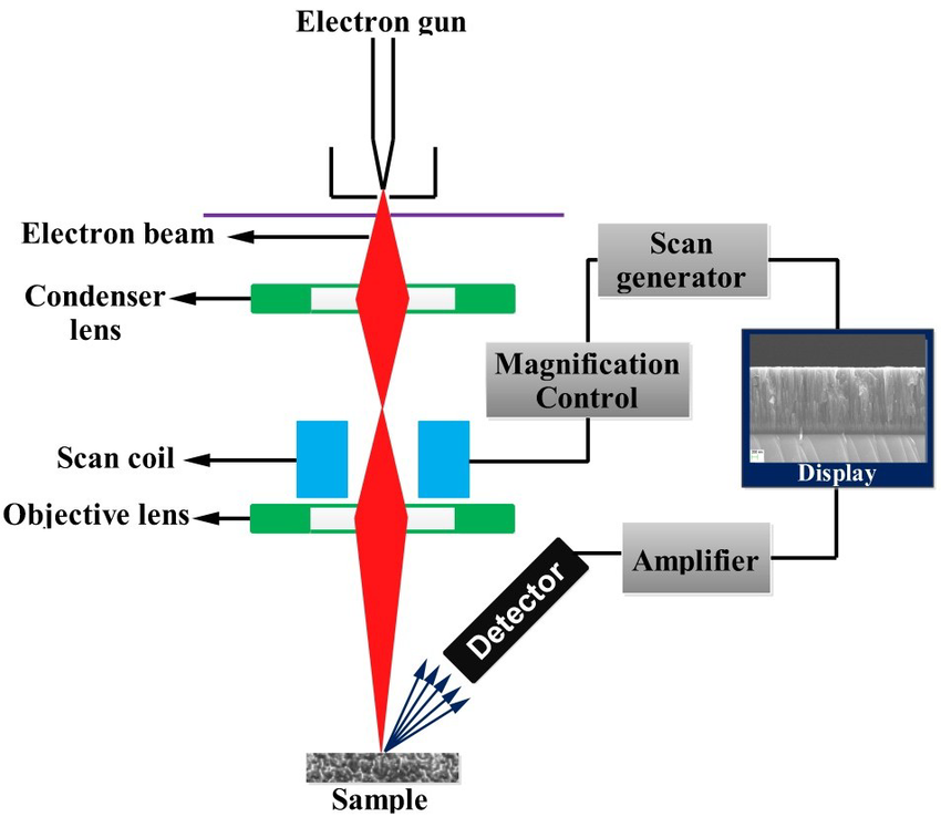
Figure 1. Schematic diagram of scanning electron microscope [1].
2.2. Structure of SEM
Taking the scanning electron microscope Hitachi S4800 as an example (Figure 2), the whole set of scanning electron microscopes is mainly composed of the electron gun, scanning signal detector, image analyzer and sample chamber. 1) Electron gun: mainly used to generate a high-speed electron beam and bombard the surface of the material to obtain sample surface information. 2) Scan signal detector: collect the material surface information excited by the high-speed electron beam. 3) Image analyzer: The collected information is recorded and processed. 4) Sample chamber: It is a vacuum device system that carries samples and electrons in scanning electron microscopy, including a sample exchange room, vacuum isolation device and vacuum detector [3].
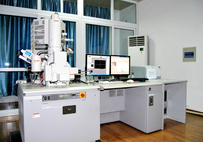
Figure 2. Scanning electron microscope Hitachi S4800 [2].
2.3. Features of SEM
The features of SEM mainly include 1) continuously adjustable magnification 2) high distinguish-ability, currently up to 1 nm; 3) strong stereoscopic image, suitable for the observation of rough and uneven fracture samples; 4) good fidelity; 5) can detect different kinds of samples; 6) with image processing and image analysis functions. Scanning electron microscopes can show various morphologies of two-dimensional materials in imaging two-dimensional materials, such as single-layer, multilayer, fold, etc. To sum up, using SEM for the study of samples includes the characteristics of fast observation, higher distinguishability, wide analysis range, more intuitive and accurate results, etc.
3. Two-dimensional materials
3.1. General introduction of 2D materials
Nanomaterials with a sheet-like morphology and huge lateral dimensions ranging between hundreds of nanometers to tens of micrometers or even larger are referred to as two-dimensional materials. So far, their typical thickness is only one atomic layer.[4]; thus, they are considered to be the thinnest chemical materials. It can be formed into heterogeneous or homogeneous structures in an out-of-plane vertical stacking or in-plane lateral splicing due to its atomic thickness and the smooth surface of 2D materials. This results in unanticipated physical and chemical properties with applications in many fields. As research on two-dimensional materials has progressed, it has expanded to include thousands of members with different electronic properties. These include insulators (hexagonal boron nitride (h-BN), mica), semiconductors (MoS2, black phosphorus, TiO2), and metals (graphene) [5]. Graphene is a two-dimensional material with an exceptional two-dimensional layered structure and superior physical, chemical, electrical, and optical capabilities. Including their electrical conductivity, light transmission, flexibility, and strength, which enable them to be used in a wide range of fields such as electronics, composites, membranes, and next-generation renewable energy technologies (e.g., solar cells) [6]. Since the mechanical exfoliation of graphene in 2004, there has been explosive growth in research on 2D materials. The unique structural characteristics and physicochemical properties of 2D materials make them one of the most attractive materials candidates across a wide range of potential applications [7].
3.2. Characteristics and preparation of 2D materials
According to the classification of different compositions of 2D materials, there are five main categories: monomers, non-metallic compounds, metallic compounds, salts and organic substances. 2D materials with different compositions exhibit properties with different functions, such as high surface area, quantum Hall effect, flexibility and superior mechanical strength. Graphene, for example, consists of a planar six-membered ring structure of carbon atoms, with adjacent carbon atoms connected by σ-bonds with a bond length of 0.142 nm and a bond angle of 120°, which Van Der Waals force interactions can stack to form graphite.
Regarding the preparation of 2D materials, the methods include mechanical exfoliation, liquid exfoliation, chemical vapor deposition and wet chemical synthesis. Among these, chemical vapor deposition (CVD) is recognized as a mature method for synthesizing two-dimensional nanomaterials. Taking graphene preparation as an example, chemical vapor deposition (CVD) is one of the most important methods for preparing large-area, high-quality graphene by using a bottom-up approach. The graphene layers prepared by this method have good controllability and conform stability regarding layer number and crystal domain size [8]. The principle of CVD is a technique for depositing materials as thin films onto a substrate by a chemical reaction composed of vapor species. Several complicated elements affect the processes and types of possible chemical reactions in a CVD reactor, including system setup, reactor configuration, gas feedstock, gas ratios, reactor pressure and gas partial pressure, reaction temperature, growth time, temperature, and so on [6]. The CVD method is widely used in the laboratory because of its ease of setup, which allows it to be used successfully in industrial settings for long periods of time and the possibility of large-scale manufacturing. In addition, the CVD method is considered one of the best ways to synthesize graphene-based materials considering ecological and cost factors [6].
Another important strategy to obtain two-dimensional materials is top-down exfoliation. The general principle is based on weakening interlayer interactions or expanding the interlayer distance by intercalating and sliding in an in-plane direction with external assistance, i.e., by exfoliating bulk layers of material to single or several layers of 2D material. The advantage of this is the ability to achieve scalable production of peeled 2D materials in a cost-effective and simple way, due to the low cost and a large number of layered precursors. In addition, the 2D material exfoliated using top-down exfoliation can be solution-processed, which may facilitate further fabrication into desired structures and applications. Despite the relatively poor quality and small cell size of exfoliated 2D materials compared to those obtained by CVD, the large increase in surface area after exfoliation using this method makes it more likely that 2D materials can be used in energy storage, catalysis, and sensing, allowing exfoliated 2D materials to be used more widely [9].
3.3. Application of 2D materials
Two-dimensional materials are widely utilized because of their special properties. These include condensed materials, biotechnology, biomedicine, biophysics, biochemistry, biomedical engineering, and other fields. For example, 2D materials can be used as electrocatalysts because of their excellent electronic properties, high surface area, good catalytic activity, and the advantage of low cost and easy preparation compared to metal-based catalysts. Further, because of their good electrical conductivity and other advantages, they can be applied to batteries or supercapacitors, energy storage, and 2D materials with good light transmission can also be used in solar cells to achieve energy conversion. It can be seen that two-dimensional materials are used in many fields.
4. Application of SEM imaging in characterizing two-dimensional materials
Scanning electron microscopy (SEM) has grown in popularity in experimental research due to the numerous benefits it offers for surface microstructure analysis and characterization. This technique has made significant breakthroughs in the structure, surface morphology, and measurement of optical properties of two-dimensional materials such as graphene, sulfides, and nitrides. These are all instances of materials that have a layered structure. SEM, for example, can be used to examine graphene's structure, imperfections, and photoelectron properties, while energy spectrometers can be used to explore aspects such as electronic transport properties and loading states. Scanning electron microscopy can be used to observe not only the multilayer structure and surface morphology of sulfides, nitrides, and other two-dimensional materials but also the photoelectric properties of the material using equipment such as energy spectrometers.
A scanning electron microscope can quickly reveal the shape and size of graphene. The image of graphene morphology shown in the figure was acquired using an optical microscope. It is clear that the surface of graphene is perfectly smooth and uniform. Image analysis shows that the graphene sample has a thickness of about 0.63 nanometers, which is consistent with the theory. This shows how the SEM measurement technique can be used in conjunction with other instruments, demonstrating SEM's versatility, dependability, and accuracy in the research realm.
Figure 3. Graphene SEM image [10].
Second, scanning electron microscopy can reveal the surface structure and irregularities of graphene. The surface of graphene has a traditional hexagonal shape and a specific lattice orientation. Graphene is a two-dimensional substance. By conducting research on these characteristics, one can acquire a better understanding and mastery of graphene's structure and properties. Furthermore, the SEM can be combined with other characterization methods to perform the multidimensional study. For example, graphene's crystal orientation has a preference, which is important information for future studies into the structure and properties of graphene. Graphene is a two-dimensional substance composed of a single layer of carbon atoms (Figure 3).
SEM, or scanning electron microscopy, is a method used in nanomaterial research to examine nanoparticles, nanowires, nanotubes, and nanostructures, among other things. The morphology and structure of materials can be visualized using scanning electron microscopy, which can generate high-resolution pictures in both two and three dimensions. The chemical composition of a material can be determined using scanning electron microscopy's energy spectrum analysis feature. (SEM). This section contains information about the material's atomic species and chemical makeup. To perform more in-depth research, SEM can be combined with other kinds of characterization techniques. For example, graphene's crystal orientation shows a degree of preference, which is valuable information for future study into its structure and properties. In addition, it is a technique that can be used to examine a wide range of nanomaterials, including nanoparticles, nanowires, nanotubes, and nanostructures. Because of the scanning electron microscope's powers, high-resolution 2D images and 3D reconstruction images can be used to show the morphology and structure of materials. The energy spectrum analysis function of the SEM can be used to identify the chemical composition of a material. This analysis can disclose details like the atomic species and atomic content.
Nanoparticles are an important subclass of nanoparticles with a wide range of promising uses. SEM can be used to study the various shapes, sizes, distributions, and crystal structures of metal nanoparticles in order to gain a better understanding of their structures and properties. Researchers can study the surface morphology and crystal structure of silver nanoparticles using scanning electron microscopy, for example. This enables them to explore silver nanoparticle biomedical and biosensor applications.
Scanning electron microscopy can be used to investigate nanomaterials. This method can be used to investigate cell surface morphology, organelle structure, and intercellular relationships. The microstructure and nanoscale details of the cell surface, including proteins, carbohydrates, and other molecules, are visible due to the high-resolution pictures obtained by SEM. Researchers can study the appearance and structure of the cell membrane using a scanning electron microscope, for example, to gain a better understanding of its role in selective permeability and cellular communication. The substructure of organelles, such as the amount and morphology of mitochondria, as well as the distribution and morphology of endoplasmic reticulum, can also be observed using a scanning electron microscope.
Further, SEM can be used to examine the morphology and distribution of biomolecules, which can then be used to explore their roles in fields such as biology and medicine. Researchers, for example, can use a scanning electron microscope to study the morphology and structure of virus particles in order to gain a more comprehensive comprehension of virus infection mechanisms and the creation of antiviral drugs. Furthermore, the scanning electron microscope can be used to investigate the structure and composition of extracellular matrix molecules like collagen, elastin, and proteoglycans to gain a better understanding of their potential uses in tissue regeneration and biomaterials. SEM is essential for studying nanoparticles and polymers. This method gives researchers a powerful tool for examining the microstructures and morphologies of the substances under investigation. These experimental examples show that the scanning electron microscope (SEM) has a wide range of uses in nanomaterials and biomaterials research. These applications provide us with a better knowledge of how these materials can be used and applied. SEM, with its high resolution, sensitivity, and spatial resolution, can be used to study material microstructures and surface morphology, as well as electrical structure, via electron reflection and transmission on the sample surface. Because of the capabilities of the SEM, these applications are feasible. Furthermore, scanning electron microscopy (SEM) is non-destructive and does not necessitate any sample surface pre-treatment on the part of the user.
However, SEM is not without flaws and limitations. To begin, SEM must be performed in a high-pressure environment, which requires keeping the surface of the sample clean to avoid contamination. SEM necessitates a higher level of scientific and practical knowledge than conventional optical microscopy. Furthermore, there are problems with SEM imaging, such as image distortion and sample degradation, that require adjustments to achieve optimum results. Finally, scanning electron microscopy (SEM) is a popular method in two-dimensional research. This method can be used to investigate the microstructures, surface morphology, and electronic characteristics of a wide range of materials. The scanning electron microscope has several benefits, including high resolution, sensitivity, and spatial resolution; however, it has several drawbacks, including sample surface requirements, technological expertise, image distortion, and sample damage. To perform thorough research and analysis with SEM, it is necessary to thoroughly examine both its benefits and drawbacks, as well as to combine it with other experimental methods.
5. Conclusion
SEM is a popular method in two-dimensional research. This method can investigate the microstructures, surface morphology, and electronic characteristics of various materials. The scanning electron microscope has several benefits, including high resolution, sensitivity, and spatial resolution; however, it has several drawbacks, including sample surface requirements, technological expertise, image distortion, and sample damage. To perform thorough research and analysis with SEM, it is necessary to thoroughly examine its benefits and drawbacks and combine it with other experimental methods.