


1. Introduction
Quantum dots have the properties of high luminous efficiency, a flexible and adjustable wavelength, and a low solution cost. Light-emitting diodes using quantum dots combine quantum dot technology with traditional semiconductor devices, showing great potential and development prospects, but there is a place for OLED to stay in the field of optoelectronics. Display screens manufactured using quantum dot technology have a wider color gamut, and using these properties, well-known companies such as Samsung and TCL are using them to manufacture displays. This article will focus on the following two issues: one is whether QLED can survive in the fiercely competitive display screen market. The other is whether OLED will gradually be replaced by QLED due to changes in technology. By analyzing the different characteristics of QLEDs and OLEDs, we can further understand the development prospects of quantum dot light emitting diodes, their market potential in light emitting diodes, and the photoelectric field [1].
2. Energy band structure and operating indicators of QLED
2.1. Atomic structure of quantum dots
Quantum dots are semiconductor nanocrystals with quantum confinement effects. Common core shell colloidal quantum dots are shown in Figure 1 (a); From the inside to the outside, the core layer (such as CdSe, etc.), shell layer (such as ZnS, etc.), and organic ligand layer (such as oleic acid, etc.) are sequentially arranged; The shell layer can passivate the surface defects of the quantum dot core, and the organic ligand can prevent the quantum dots from agglomerating, making them stable in the system; The core shell structure ensures the high luminous efficiency and stability of quantum dots[2].
The low-dimensional semiconductor material known as the quantum dot is notable. It is not more extensive than twofold the excited state Bohr radius of the analogous semiconductor component in three dimensions. The radius of quantum dots can generally be spherical or quasi-spherical, which oscillates between 2 to 20 nm. Common quantum dots are created by combining from layers IV, II-VI, IV-VI, or III-V. It is believed that there are multiple instances of the so-called quantum dots, such as silicon, germanium, cadmium sulfide, cadmium selenide, cadmium telluride, zinc selenide, lead sulfide, lead selenide, indium phosphide, and indium arsenide quantum dots that exist [3].
.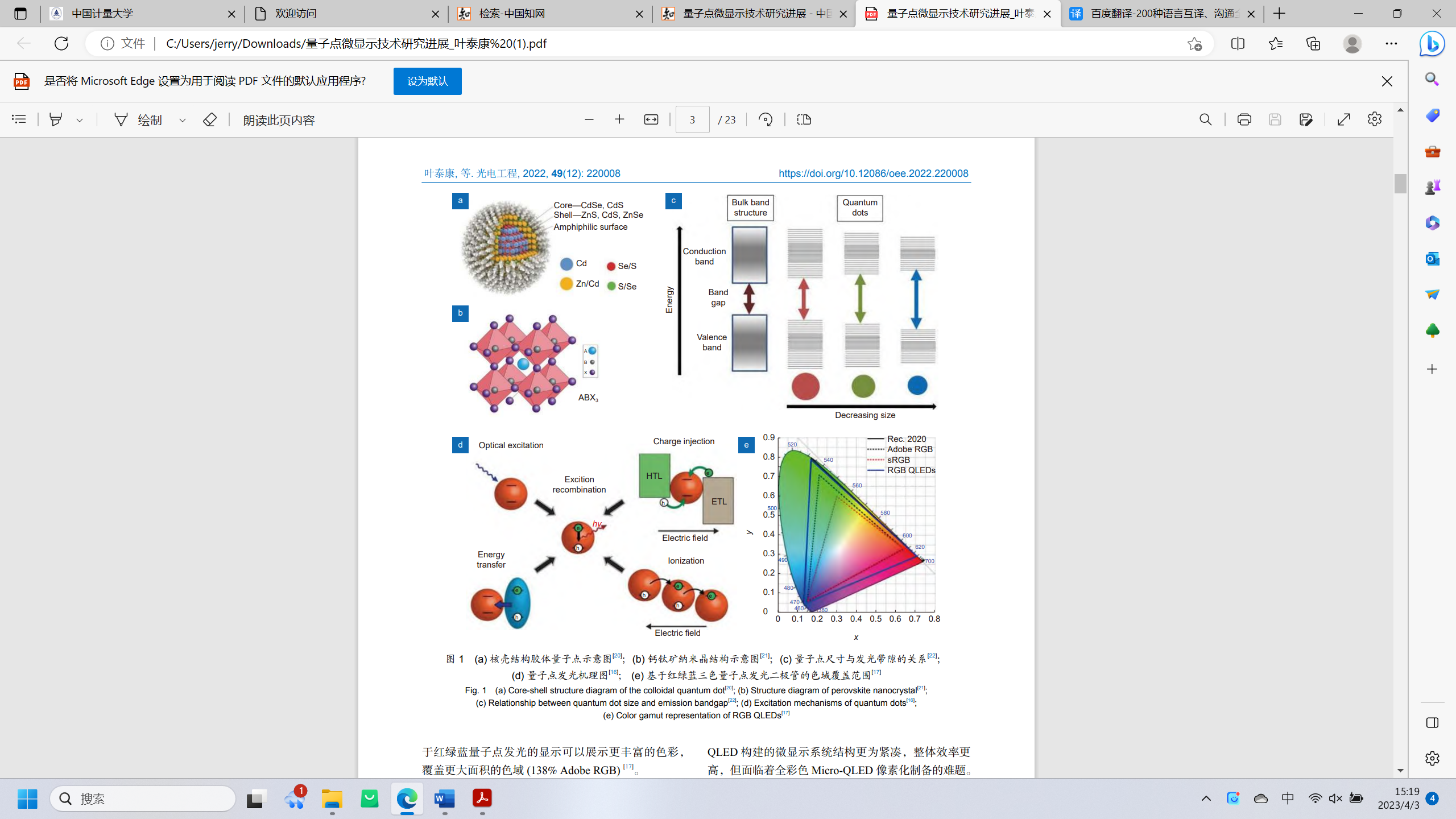
Figure 1. Core-shell structure diagram of the colloidal quantum dot.
2.2. QLED’s energy band
Figure 2 illustrates how a compatible electrical conduction band minimum (CBM) of a mixture of zinc oxide (ZnO) and quantum dot (QD) effectively implements electrons into the radiation emission layer (EML) to form excitons, thereby benefiting from the hole transport layer's hole-coulomb interaction. (HTL). To explicitly hypothesize and guarantee the infusion of charge at junction situations by setting based CBM alone, however, proves difficult owing to the stoichiometric and crystalline defects in ZnO which may take place in sub band gap states. In addition, the asymmetric charge injection and transmission between ETL and HTL make it difficult for these devices to achieve optimal electroluminescence performance [4]. Lack of a robust and adequate comprehension of these layout behaviors frequently ends in incoherent draws when striving address issues with performance to QLED.
Figure 2. Energy level diagram of the QLED.
In simple terms, the oxygen layers represent the biggest part of the QLED's energy band structure. With regard to Figure 3, The intermediate energy band (Oii) belongs to electronic states related to oxygen vacancies, whereas the highest and lowest energy bands (Oi and Oiii) have a connection with glycolic and ionized oxygen ions, respectively. In straightforward terms, oxygen-rich layers constitute the main element of the QLED's energy band structure. Bearing in mind Figure 3, The intermediate energy band (Oii) has a correlation to states of electronic structure related to voids in oxygen, whereas the highest and lowest energy bands (Oi and Oiii) are linked with acid and ionized breathable air ions, respectively.
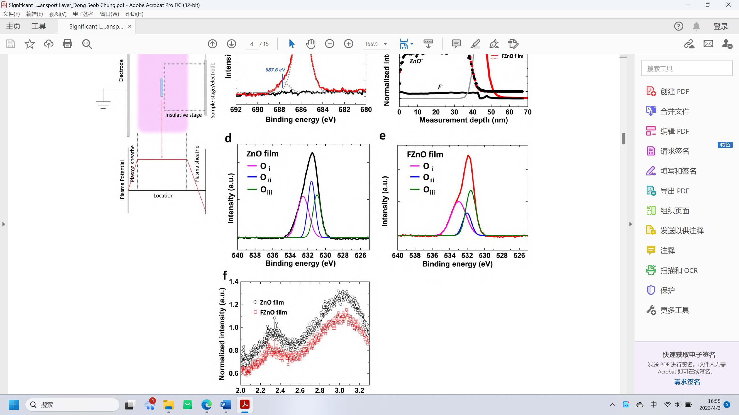
Figure 3. 1s core level electrons in ZnO flm and FZnO flm.
2.3. QLED’s performance indicators
The entire spectrum of shades that an electronic system is able of yielding can be referred to as the "color gamut," which serves as a method of categorizing a color. Color gamut is a broad subset of colors utilized for computer graphics processing. The most prevalent application of color certain segments is to authentically portrayed an individual condition. This could include an existing color space or an output device's color breadth [5]. The reason why color gamut can be an operating indicator is that it can measure different sorts of colors and QLED can produce lots of colors, making it easy to evaluate the quantities of QLED’s producing colors to ensure quality.
When convinced photons impact the outermost layer of a photosensitive device, the photosensitive material becomes excited to form electron hole pairs, which leads to in an electric current [6]. The ratio of all incident photons to all of the electrons acquired through methods like internal electron-hole recombination is known as the external quantum efficiency. (Mainly called EQE). The ratio of the number of photons output in the plane per unit time compared to the number of pairs of electrons and holes injected in the plane according unit time is used to measure the external quantum efficiency of light-emitting diodes [7].
3. Comparison of quantum dot light emitting diodes and organic light emitting diodes
3.1. Organic light emitting diodes (OLED)
A substrate, a cathode, an anode, a hole injection layer (HIL), an electron injected layer (EIL), a hole transport layer (HTL), a layer for the transport of electrons (ETL), an electronic barrier layer (EBL), a hole barrier layer (HBL), a light emitting layer (EML), etc. constitute the components of OLED devices. All functional layers may be steamed on the device's base plate, which doubles as the device's skeletal core. The basis plate for devices can frequently be made of glass, however if adaptable OLED devices must be manufactured, alternative materials, such as plastics, are needed. The electrode that receives the majority of the instrument's external drive voltage is connected to the anode. Under the influence of the exterior drive voltage, the anode's holes will travel to the device's light-emitting layer. In order for the light emitted throughout the device to be visible to the outside when it is operating, the anode must be permeable to certain degree. Indium Tin Oxides constitute the most widely used material for the anode. (ITO). The device's anode can be tweaked using the cavity injection layer, facilitating a smooth injection of the device's anode's cavity into the reservoir transport layer. The voids can only be transmitted to the illuminated layer as the void transport layer. The power source barrier layer increases the concentration of electrons at the interface of the device's light emitting layer by prohibiting electrons from the cathode at that particular location. The shining layer is the point where the device's electrons and holes connect with again in order to generate an exciton, which afterwards declines in order to activate the light. With the goal to boost both the potential for recombination of electrons and voids at the interface of the device luminescent layer and the luminescent efficiency of the device, the void obstacle layer separates the voids from the anode at the interaction of the device luminescent layer. The device's electron transport layer is in charge of electrons in motion from the cathode to the layer that emits light. The particle injection layer serves as an electron transfer and cathode modification layer. The external environment drive voltage of the device propels the electrons in the cathode area toward the light-emitting layer of the device, where they merge with the holes form the anode [8].
3.2. Quantum dot light emitting diodes (QLED)
The key difference between OLED technology and the quantum dot light-emission diodes (QLEDs) is that the luminescent component of QLEDs is comprised of a mixture of quantum dots alongside different supplies. Its structure is with the result that in the quantum dot layer, electrons and holes from both sides unite in order to generate photons (excitons), which then reunite to form light.
Quantum dots refer to semiconductor nanocrystals with particle sizes smaller than or close to the Bohr radius of excitons. The scale of the three dimensions of a quantum dot is usually below 10nm, and the movement of electrons and holes inside is restricted in all directions, resulting in a significant quantum confinement effect. Quantum dots used in the field of luminescence generally have a core-shell structure and their surfaces are passivated by ligands. Quantum dots characteristic various energy level structures mainly become the outcome of the quantum isolation of the electrons and holes. Through their respective positions distinct energy level structure, quantum dots display special spectral properties. Quantum dots illuminate whenever they are triggered by light or electricity, and the materials and size of the quantum dot shape the energy wavelength of the fluorescence. This characteristic allows quantum dots to change the color of the light emitted by the light source. Quantum dots have narrow emission peaks, adjustable emission colors with their own size, and high emission efficiency, making them very suitable as luminescent materials for display devices. The half peak width of quantum dot emission is about 30 nm, while the half peak width of traditional organic molecule emission is about 100 nm [9].
Compared to OLED, QLED has advantages such as higher theoretical luminescence efficiency, tunable color, wider color gamut, better color saturation and brightness, and a lower energy consumption cost, making quantum dot electroluminescence technology a favorable candidate for the next generation of new display technologies.
4. Preparation technology of quantum dot light-emitting diodes
4.1. Lithography technology
Prepare a layer of polyvinyl pyrrolidone (PVP) as a sacrificial layer in advance on the substrate, then spin coat the photoresist for exposure and development to form a pattern. ICP etching is used to remove the sacrificial layer without photoresist protection, then quantum dots are added, and finally the surplus quantum dots and photoresist are removed from the sacrificial layer. Sacrificial layers also make the process of removing photoresist simpler, which lessens the impact of the photoresist stripping procedure on quantum dots during the lithography process. Finally, the pixel density of Micro QLED prepared in this way can reach 500 ppi, breaking the pixel density record of full color Micro QLED at that time. Micro QLEDs determined by the three types of quantum dots have peak brightness of 108,000, 247,000, and 340 nits, respectively, with current efficacy of 8.3, 9.8, and 0.02 cd/A, for each [10].
4.2. Spray printing technology
Quantum dot film is prepared by spray printing. The uniformity of the film will largely determine the display effect. During the spray printing process, when a single ink droplet evaporates and dries on the base, an uneven accumulation of quantum dots, i.e., the coffee ring effect, often occurs. This will have a direct impact on the quantum dot race conversion layer's uniformity, which will subsequently have an impact on the display effect. The coffee ring phenomenon tends to be brought on by the marginal evaporation rate being higher than the central evaporation rate. This causes blood to circulate from the interior of the puddle to the edge area surrounding the droplet, resulting in a buildup of quantum dots on the edge. Based on its formation mechanism, capillary flow can be balanced by either inhibiting capillary flow or using Marangoni flow. This reduces the coffee ring effect and improves the uniformity of the quantum dot pattern [11].
5. Conclusion
Quantum dots have advantages such as high luminescence efficiency, an adjustable luminescence bandgap, a narrow luminescence half peak width, and low-cost preparation by the solution method, which can be applied in many display application scenarios. The implementation of full color, high brightness, and high pixel density micro displays required for the increasingly popular near eye display scenarios remains a huge challenge. Quantum dot light-emitting diodes (QLEDs) are stronger than organic diodes (OLEDs) in many aspects, have a foothold in the photoelectric field, and have great potential for the development of photoelectronic devices. However, the stability of QLDs still needs to be adjusted, and their IQE (internal photoelectron acceptance efficiency) is lower. By increasing the EQE (external photoelectron acceptance efficiency), we can make up for the loss of EQE-and further improve and perfect the preparation method. In the future, we can explore the quantum dot display and apply it to large quantum dot displays from TV screens to mobile screens-and computer screen development and expansion. Quantum dots, as a representative of breaking through traditional luminous materials, have a wide application prospect in the fields of optical communication and display lighting-and have been widely studied. In recent years, the synthesis and fabrication of quantum dots and optical devices have been greatly developed. The efficiency of silicon quantum dots and their devices has been continuously improved by new means and mechanisms.