

1. Introduction
Field-effect transistors (FETs) have witnessed significant advancements since 2000. The development of high-k dielectric materials, Fin-FET and nanowires lead to improve gate capacitance and electrostatic control. As FET dimensions have continued to scale down, better transistor densities and enhanced performance have been made possible [1]. Figure 1 displays a diagram of a FET in the actual world [2]. It is a three-terminal semiconductor device that has several different uses, including switching and amplification. The modulation of an electric field generated by a Gate electrode on the flow of current via a semiconductor channel between two further terminals, known as the Source and the Drain, is the basis for a FET's operation. An electric field that is produced when a voltage is supplied to the gate terminal regulates the passage of current through the channel.
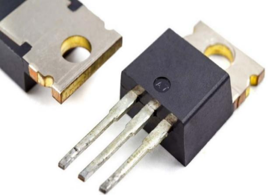
Figure 1. The real word photograph of the FET [2].
Compared to other types of transistors, including bipolar junction transistors, FETs have several benefits (BJTs). For instance, FETs require less current from the input signal source because they have higher input impedance. Moreover, they respond more quickly and are less prone to thermal runaways. Several different electrical applications, such as audio amplifiers, RF circuits, power supply, and digital circuits, make use of FETs. They are a crucial element of contemporary electronics since they are utilized in several integrated circuits (ICs) and microprocessors. The general operation of FETs and the many varieties of FETs will be covered first to acquire these qualities. Besides, some new techniques will be shown later on.
2. The mechanism of FETs
2.1. The principal operation of FETs
Using an electric field, a FET controls the current flow between its source and drain terminals. The voltage provided to the gate terminal, which modifies the electric field in the channel, regulates the current flow. An electric field between the source and drain terminals is produced in the channel of a FET when a voltage is supplied to the gate.
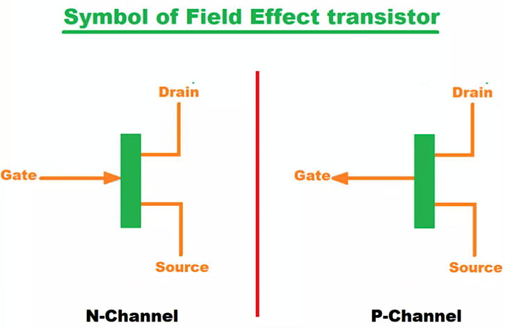
Figure 2. Symbol of a field effect transistor [3].
The letters D, G, and S are represented on the diagram by the gate, source, and drain terminals. As seen in Figure 2, the arrowhead's orientation corresponds to the electric field's direction. The different electric field directions change the current direction. By the main operation, the FET will be in one of two functional states: N-channel or P-channel. The N-channel FETs have P-type source and drain regions. When a positive voltage is applied to the gate, enabling electrons to flow across the channel from the source to the drain, the device is referred to as being in the "on" state. When the gate voltage is lowered, its channel becomes less conductive, and the device switches to the "off" state. On the other hand, N-type source and drain regions are present in addition to the P-type channel in P-channel FETs. The gadget "turns on" when holes travel from the source to the drain across the channel when the gate gets a negative voltage. When the gate voltage is increased, the device goes into the "off" state because the channel loses conductivity [4].
As shown in Figure 3, the canal is exhausted by a N channel FET, where electrons are the main charge carriers. The electrons would be taken from the gate if it were made more negative, saturating the channel and increasing its resistance. The gate area thins because of the decreased electron traffic, yet the conduction channel is said to be depleted as a result of the increased resistance.
Figure 3. The functioning schematic for a FET [5].
2.2. The types of FETs
2.2.1. JFET. The junction gate field-effect transistor (JFET) is a voltage-controlled transistor, whereas a regular transistor is a current-controlled device that requires current for biassing. The three terminals on a JFET are identified as Gate, Drain, and Source. It is also offered as an N- and P-Channel JFET. It is an essential component for analogue electronics' precision-level voltage-operated controllers. JFETs can be used to create switches, voltage-controlled resistors, and amplifiers. Additionally, it features a BJT replacement version that uses less energy. JFETs have relatively low power dissipations, which raises the circuit's overall efficiency.
| Figure 4. (a) The simple diagram of the structure JFETs and (b) The construction of the N-Channel and P-Channel JFETs [6]. |
(a) | |
| |
(b) |

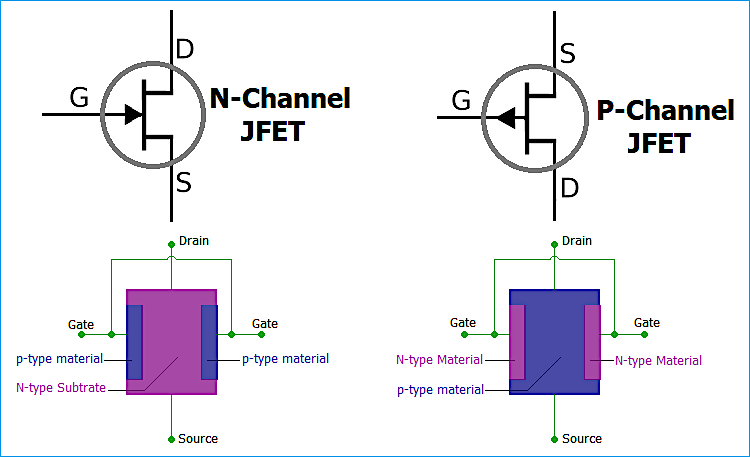
The P-Channel JFET is made up of N-type materials in a P-type substrate, as opposed to the N-Channel JFET, which is made up of P-type materials in an N-type substrate. JFETs are built utilizing a long channel of semiconductor material, as seen in Figure 4. According to the construction method, a JFET is referred to as a P-type JFET if it has a high concentration of positive charge carriers (also known as holes), and an N-type JFET if it has a high concentration of negative charge carriers (also known as electrons). The Source and Drain connections are made by creating Ohmic contacts at each end of the long channel of semiconductor material. A P-N junction develops on either or both sides of the channel.
2.2.2. Metal-oxide-semiconductor field-effect transistor (MOS-FET). MOS-FET is a kind of field-effect transistor (FET) that uses a metal gate electrode on top of an insulating layer (silicon dioxide) to regulate the movement of current via a semiconductor channel between two additional terminals known as the source and the drain. The MOSFET is a three-terminal electrical component that is frequently employed as a switch or amplifier in circuits. There is a capacitor between the metal gate electrode and the semiconductor channel because there is a thin insulating layer between them. By applying a voltage to the gate, the electric field created by the gate voltage modifies the conductivity of the channel, allowing or blocking the flow of current between the source and the drain. As MOSFETs are the FETs that are most commonly used, we will utilize these components to explain the structure and functionality of this group of transistors. The components of a typical MOSFET, where the transistors are constructed on the surface of a silicon bulk substrate, are shown in Figure 5.
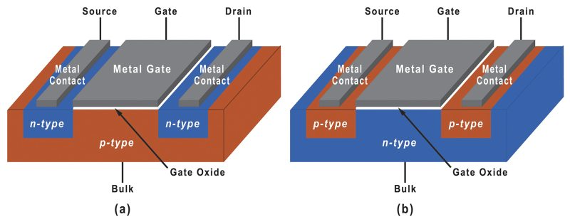
Figure 5. (a) NMOS and (b) PMOS [7].
According to the polarity of the bulk, source, and drain regions, MOSFET can be constructed as either NMOS or PMOS transistors, as shown in Figure 5. In NMOS devices, electrons predominate over charge carriers, whereas in PMOS devices, holes predominate over charge carriers. As shown in Figure 5, NMOS devices are constructed on p-doped silicon substrates and N-type material areas are created using ion implantation (a). It refers to the source and drain of these n-type regions. As seen in Figure 5, the situation is the opposite in PMOS devices (b). The channel is the term for the mass of material that lies between the MOSFET source and the drain. The channel region is covered by a very thin insulating oxide layer. Gate oxide is the term used for it. To create the three-terminal device structure, the conductive gate material is ultimately placed on top of the gate oxide. This material can either be metal or highly doped polysilicon [7].
2.2.3. Carbon nanotube (CNT) -FET. As technology advances, new types of FETs are created using more effective materials. Consider a FET made of CNTFET. The carbon nanotube used in this FET is sandwiched between the source and drain electrodes, which are connected to the gate electrode and kept apart from the nanotube by a thin insulating layer. It can be further separated into the four sections depicted in Figure 6.
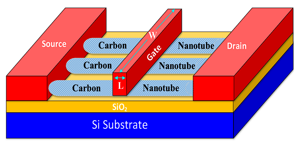
Figure 6. The schematic of a type of CNTFET [8].
Source and Drain Electrodes: The carbon nanotube is connected to the electrical system through these metallic connections. At either end of the nanotube, they are often constructed of a metal like gold or platinum. The most important component, the carbon nanotube, acts as a conducting path between the source and drain electrodes. It is an anometer-diameter-diameter cylindrical form of carbon.
The gate electrode is a metallic contact that is placed in front of a carbon nanotube and is isolated from it by a thin, silicon dioxide-based insulating layer. The gate electrode generates an electric field that affects the carbon nanotube's ability to conduct charge carriers (such as electrons or holes).
The insulating layer keeps the carbon nanotube and gate electrode from coming into direct electrical contact. Typically, silicon dioxide or other insulating compounds are used to make it. The insulating layer of the CNTFET in Figure 6 is made of silicon dioxide.
3. The challenges that FETs face
3.1. Short channel effect
When the transistor channel is shortened to the point that the depletion zones surrounding the source and drain regions start to overlap, the short channel effect happens. The depletion region moves further into the channel as the length of the channel shortens due to a greater electric field at the drain end of the channel. This depletion region can restrict the current flow and cause a reduction in the drain current, known as drain-induced barrier lowering (DIBL). Another effect of short channel length is channel-length modulation, where the depletion region at the drain end of the channel interacts with the gate electric field, causing a change in the effective channel length. This effect can result in a decrease in the output resistance and a reduction in the voltage gain of the device.
3.2. Gate-induced drain leakage (GIDL)
Current flows from the drain to the source even when the gate voltage is zero due to a phenomenon known as GIDL in FETs. A leakage current that travels through the gate oxide and into the FET's channel is what causes GIDL. Modern FETs, especially those with thinner gate oxide layers, are susceptible to considerable current leakage via GIDL. Increased power loss and decreased device dependability may result from this. Reduced on/off current ratios caused by GIDL can impair FETs' ability to flip between the on and off states, which can have an impact on their performance. Interface states in the gate oxide, trap-aided tunnelling, and carrier production in the drain depletion zone are some of the variables that might cause GIDL. The use of thicker gate oxides, a decrease in the amount of doping in the drain region, or the addition of additional process stages to lower interface states is all options for device designers to reduce GIDL [9].
3.3. Contact resistance
It still has various faults and problems because it is a novel type of material utilized in FETs. For instance, one of the key issues with CNTFETs is contact resistance. It may restrict the amount of current that can pass through the gadget, which would lower performance. The metal source and drain connections found in CNTFETs are in direct contact with the CNT channel. It is difficult to create a low-resistance electrical contact between the metal electrodes and the CNT because the CNTs are so tiny, often having diameters of only a few nanometers. In other words, due to the CNTs' small size, the metal electrodes might not be able to make good electrical contact with them.
Due to the chemical makeup of the metals utilized, the metal-CNT interface may also experience high contact resistance. For instance, the chemical interaction of particular metals with the CNTs or the formation of a barrier layer at the interface can considerably raise contact resistance. Numerous problems, including increased power consumption, slowed signal speed, and changes in device characteristics, might result from high contact resistance. To improve the electrical contact between the metal electrodes and the CNT channel, researchers are actively striving to discover innovative techniques to lower contact resistance, such as employing other metals or changing the CNT structure.
4. The possible solutions
4.1. DIBL
To reduce short-channel effects, a unique form of CNTFET was created. Stepped Lightly Doped Drain and Source (LDDS)-CNTFETs are the name given to them. The leakage currents of carbon nanotube base transistors (C-MOSFETs), LD-CNTFETs, and LDDS-CNTFETs are significantly reduced by contrasting the stepped and light impurity structure in the drain and source regions with the base structure, linear impurity structure in the drain and source regions, and light impurity structure in the drain and source regions. This is caused by the presence of impure drains and drain-style sources, which increase the barrier between the drain and source regions and reduce the likelihood of band-to-band tunnelling. Comparative drain currents for the various topologies are shown in Figure 7 for drain-source voltages of VGS = 0.3 V and VGS = 0.4 V. The ions of the proposed structure are larger than those of the other structures for a given gate-source voltage [10].
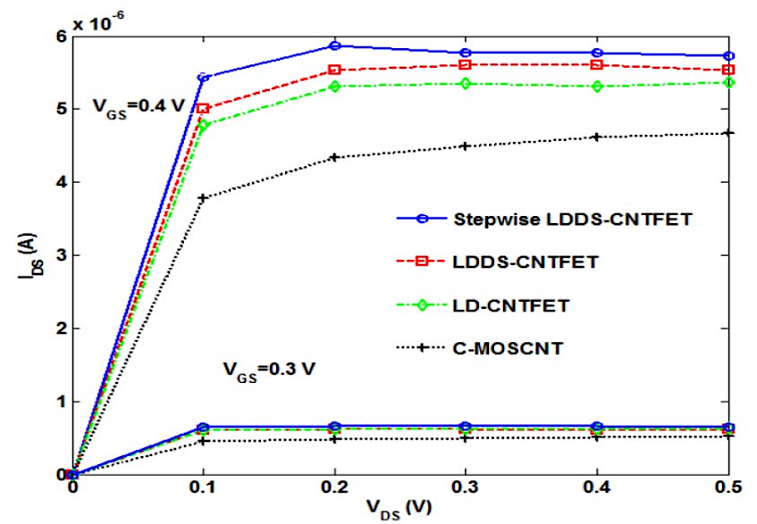
Figure 7. Drain current diagram of different structure FET at different gate-source voltages [10].
4.2. GIDL
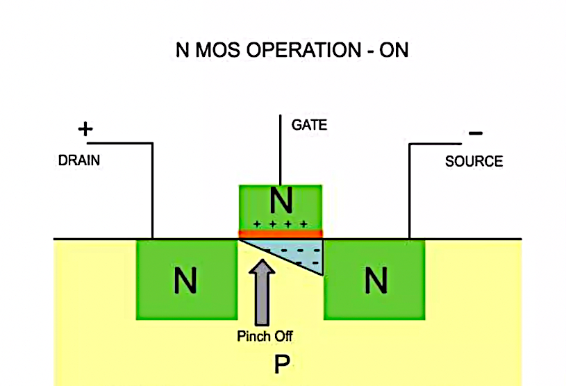
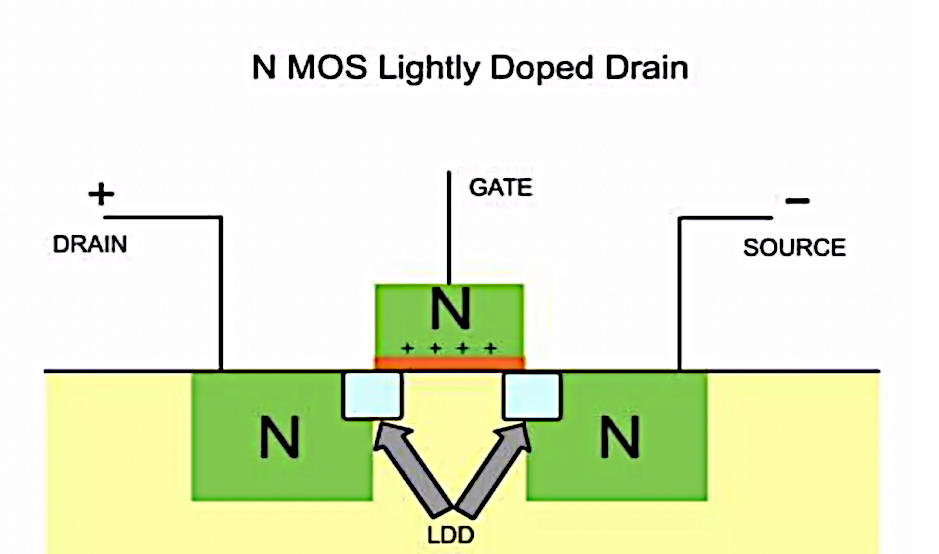
Using a Lightly Doped Drain is one of the most effective techniques to reduce GIDL or the hot electron effect (LDD). The drain area close to the channel is doped less than the main drain area as part of LDD's effort to reduce the hot carrier effect. The LDD in the MOSFET lowers the doping concentration at the junction of the reverse-biased drain and channel. The depletion breadth at this juncture widens as a result. Consequently, the electric field can be diminished (Figure 8).
|
|
(a) | (b) |
Figure 8. (a) the normal N-Channel MOSFET and the pitch-off effect; (b) the difference when the LLD is used in the transistor. LDD plays an important role as it greatly improves the N MOSFET [11]. | |
4.3. Doping
The contact resistance in carbon nanotube field effect transistors (CNT-FETs) between the CNT channel and the metal electrode is a significant problem that can be solved by chemically doping the CNT-CNT. Chemical doping of CNT-CNTs involves the use of particular chemicals to dope the CNT channels. This can alter the CNT's electrical characteristics and lower the contact resistance between the CNT and the metal electrode. Methylene dithiol (DMT), one of the often-employed compounds, can create covalent connections between CNTs, effectively lowering the contact resistance between them. The following are the precise stages of CNT-CNT chemical doping:
1. The CNT channel is injected into the metal electrode of the CNT-FET device, bringing it into close contact with the electrode.
2. Between the CNT-CNT is inserted a substance containing DMT.
3. The Sulphur atoms in the DMT molecule form a covalent bond with the carbon atoms in the CNT-CNT, forming a chemical bond connection.
4. The formation of this chemical bond reduces the contact resistance between the CNT-CNT, thus improving the performance of the device.
The concentration of the dopant and the reaction time must be controlled during the CNT-CNT chemical doping process to prevent over-doping and deterioration of device performance. The scheme's viability and whether it produces such effective effects are still debatable.
5. Conclusion
The fundamental workings of FETs were primarily covered in this article. To determine the benefits and drawbacks of each type of FET, it also compares MOSFET and JFET. Some solutions to the problems are also becoming available. Through the replacement of the original drain with a LDD, the pitch-off impact on the N-Channel MOSFET can be lessened. Additionally, it introduces the CNTFET and OFET, two novel FETs. New materials and organic chemical techniques are used to increase the size and efficiency of these new FETs. According to the research, creating novel metal-oxidized or organic polymer compounds will broaden the uses of transistors for the general population, though challenges still lie ahead. Moreover, because of the lack of equipment, current knowledge and means, some of the properties cannot be tested. For instance, there is only an improved method to use CNT-FET but unable to test its efficiency. Due to the high-tech required, future FET may be smaller in size, less cost, have a more advanced work function and also use in numerous places around the world.