


1. Introduction
The advancement of science and technology has led to the generation and exchange of data becoming one of the most significant driving forces for social development. The fields of satellite remote sensing, mobile communication, and cloud computing, among others, require the transmission of a considerable amount of data. [1] Nevertheless, with the exponential growth in the volume of data, concerns about data security and the efficiency of data transmission have become increasingly pressing.
In the field of communication, the past decades have seen a significant focus on the design of scrambling and decoding circuits. A number of highly efficient scrambling algorithms and some advanced decoding algorithms have been developed, which can effectively improve the stability and security of the data transmission process. Nevertheless, further research is still required to ascertain how to reduce the BER, how to process large data streams, and how to achieve data security.
In this study, the linear feedback shift register (LFSR), as the main component of the scrambling module, can effectively improve the efficiency and security of data transmission. The hardware implementation is simple, it consists of one shift register and several logic gates. It can quickly generate a large amount of data at high-speed frequency. Its generated sequences have good randomness and predictability, which can improve data transmission security [2]. Meanwhile, based on specific initial state and feedback polynomials, LFSR can generate output sequences with fixed periodicity, which ensures the predictability and repeatability of the sequences [3].
The design and implementation of scrambling and decoding circuits typically require the use of a variety of tools. For example, Verilog or VHDL programming languages are commonly used hardware description languages for writing logic code for scramblers and decoders. FPGA development boards provide hardware platforms for verifying and testing circuit designs, allowing designed circuits to be loaded onto actual hardware for real-time testing and verification. EDA tool suites are used to design, simulate, and verify circuits. Simulators and simulation tools such as ModelSim can be used to verify the functionality of the circuit design. These tools are essential for designing and implementing efficient and reliable scrambling and decoding circuits.
When designing a communication system, it is often assumed that the probability of a “0” and a “1” occurring in the transmitted bit stream is 50/50. To ensure communication quality, the occurrence of consecutive “0” or “1” codes in digital baseband transmission must be reduced to ensure recovery quality. However, the encoded transmission stream may contain consecutive “0s” or “1s”, causing the system to fail to meet the designed performance specifications. To overcome these problems, the data stream is often scrambled before entering the transmission channel to limit the length of consecutive “0s” or “1s” by converting the binary digital information into a pseudo-random sequence [4].This encryption is often referred to as “scrambling”. The process of unscrambling at the receiving end is called decoding.
The experimental verification method is to simulate the designed circuit, so the following assumptions must be made for this circuit: The transmission medium is assumed to be ideal, i.e., the effect of the transmission medium on signal attenuation, noise is not taken. Assume that the clocks at the transmitter and receiver are perfectly synchronized, with no clock offset or jitter. It is assumed that the components in the circuit are ideal and that there are no non-linearities, or distortions.
During the simulation of the scrambling module, it should be possible to observe that the input data is scrambled. In the decoding module, the result is seen when the information is consistent with the original data. If all the conditions are met, it is anticipated that the circuit will successfully scramble and recover the original data from the scrambled data with no signal loss or distortion.
In conclusion, the evidence presented in this study demonstrates that the linear shift register is a viable and efficacious method of scrambling and decoding. The simplicity of its hardware implementation and the speed of its operation enables it to generate large amounts of data in a short period of time, thereby improving the efficiency and security of data transmission. These findings validate the importance of scrambling and decoding techniques and foretell their great potential in the field of data transmission in the future.
2. Scrambling and decoding hardware architecture design
The circuit architecture of scrambling and decoding is shown in fig 1. The receiver and the transmitter have the same structure, and the circuit structure is simple, consisting of multi-stage flip-flops and two-input XOR gates. The basic operation principle Takes the transmitter as an example, the original data is transmitted into all flip-flops, and the flip-flop sends the output data into the next flip-flop or XOR gate. The XOR gate will re-input the processed data into the trigger, and the final output scrambled data will be different from the original data or form scrambled data. It is easy to know that the scrambled data will be different from scrambled data again and the original data can be obtained again [4]. The hardware architecture of the circuit is composed of four parts, including a scrambler module, decoder module, control module, and data input and output module. The scrambler module, decoder module, and control are composed of multi-stage flip-flops and XOR gates [5]. This circuit can be used to generate the longest linear feedback shift register sequence, that is, an m-sequence [6].
Figure 1. Scrambling decoder structure diagram.
3. Module division submodule implementation
In scrambling and decoding circuits, the core functional components are the scrambling module and the decoding module, which are essentially linear shift registers (LFSRs). These are implemented by a set of shift registers and a feedback network of a variety of heteroscedastic logic gates. The LFSRs require an initial state to be provided, which is populated with an initial value through the initialization module. After this, the LFSRs are shifted once for each clock pulse, with each register’s value shifted one bit to the right and into the new register. During each shift operation, a variety of register operations are computed, generating a new bit and being entered into the leftmost register. The repetition of the operation results in the generation of a pseudo-random sequence [7].
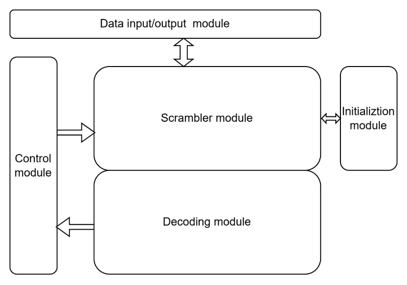
Figure 2. Module division Submodule implementation.
The data input module is responsible for feeding the raw data into the scrambler module, while the data output module is tasked with sending the decoded data out. The control module is responsible for regulating the operational state of the circuit. The control module is employed to regulate the operational state of the circuit, encompassing functions such as initiation and termination, as well as resetting. The initialization module serves to initialize the LFSR during the startup or reset of the circuit, in fig 2.
4. Simulation
The simulation works roughly as follows: for each clock pulse, if the shift register is shifted one bit to the right, one bit is left on the left side of the shift register. If there is an input on the left, there will be a steady stream of output data on the right output of the shift register. If one sequence from a shift register forms a left-hand input based on a certain feedback function, then the structure is called a feedback shift register. When the feedback function of a feedback shift register is linear, it is finally called a linear feedback shift register. The feedback function of a linear feedback shift register is to XOR some bits in the shift register. The linear feedback shift register is obtained by feeding the computational result of the feedback function to the far left of the shift register, and the output of the last flip-flop is a pseudo-random sequence [8].
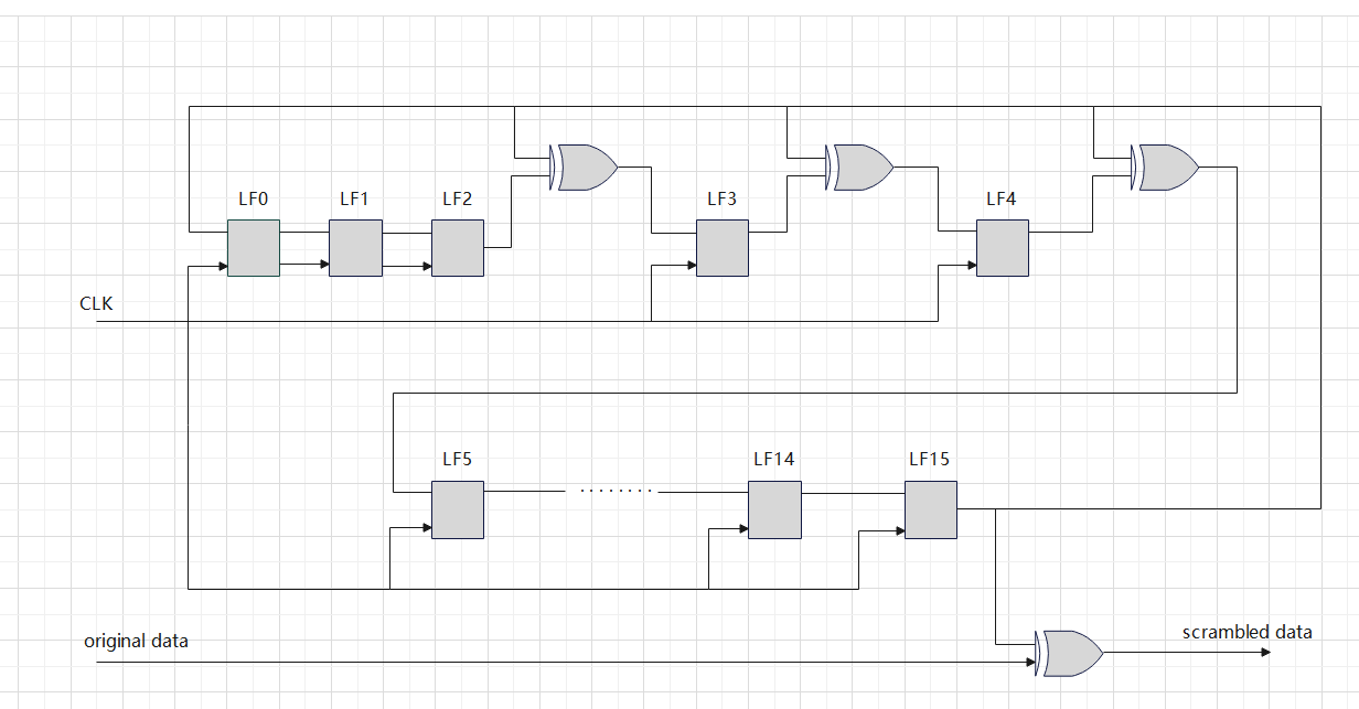
Figure 3. 16-Level linear feedback shift register.
This circuit diagram uses a linear feedback shift register and XOR gates to scramble the input data in fig 3. There are 16 LFSR units in the circuit components, ranging from LF0 to LF15, and each one is represented by a flip-flop. The LFSR is driven by a clock signal, moving its contents bit by bit. There are multiple XOR gates in the circuit, which are used to implement the feedback function of the LFSR and the scrambling of the input data [9].
The fig 4 shows the structure of the LFSR with the primitive polynomial x^16 + x^15 + ...... + 1 [10]. It consists of 16 levels of flip-flops, where the input of D1 is the result of the output XOR of D3 and D2, and the output of O2 is a pseudo-random sequence with periods of 2^16 - 1 = 65535.
5. Simulation results
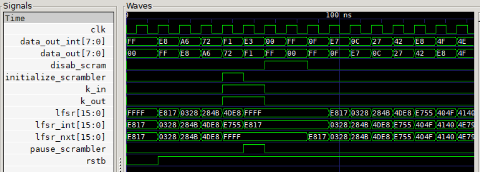
Figure 4. Scrambling decoding the simulation of the entire circuit.
This experiment designed a verilog code for an 8-bit scrambler and decoder and wrote the corresponding testbench code for simulation testing.
In the first test case, the scrambler is provided normal data, and the output is observed. After simulation verification, the scrambler can correctly scramble the input data and transmit the results to the decoder. The decoder is able to decode correctly and recover the original data.
The second test case simulates the case of sending control characters, such as COM characters and SKP characters. By setting specific input data and control character flags, it is possible to verify that the scrambler and decoder can handle these control characters correctly and do not scramble or decode them.
In the third test case, the ability to disable scrambling code is tested. By setting the disabling scrambling flag, it can be seen that even if normal data is received, the scrambler does not scramble the code but transmits it directly to the decoder.
The last test case tests the ability to re-enable scrambling. In the case of previously disabled scrambling, re-enable scrambling and observe the output. The simulation results show that the scrambler restarts scrambling the input data, and the decoder can decode the data correctly.
Through the simulation tests above, the normal operation of the designed scrambler and decoder in various situations is successfully verified. These simulation results prove the correctness and reliability of its functions, and provide a reliable basis for the design and implementation of digital communication systems.
6. Conclusion
This paper mainly studies the design and implementation of scramble and decoder circuits. Through the analysis of the principle of scramble and decoder, an efficient scramble and decoder circuit is designed, and the possible results are predicted according to some idealized assumptions and verified by experiments. Through in-depth analysis and understanding of the working principle, the security of data transmission can be guaranteed. Although there is a gap between the ideal assumption and the actual situation, researchers still hope to see more stable scrambler and decoder circuits designed. In the future, researchers can see more complex and efficient scrambling and decoding schemes proposed, which may have more advanced techniques. At the same time, with the optimization of the existing coding technology, researchers expect to have a more efficient decoding process, reduce errors, and improve the data recovery rate.
Authors Contribution
All the authors contributed equally and their names were listed in alphabetical order.