


1. Introduction
Hybrid perovskite solar cells (PSCs), named after the crystal structure of the light absorber and the mineral CaTiO3, have emerged as a novel class of photoelectric semiconductor materials in recent years. Due to their inherent strong light absorption capacity, high low-light efficiency, as well as cost-effectiveness and ease of preparation, they present a promising alternative to commercially available silicon-based solar cells.
Hybrid halide perovskites were initially employed in photovoltaics in 2009 as sensitizers, replacing dye pigments in dye-sensitized solar cells (DSSCs), achieving an optimal power conversion efficiency (PCE) of 3.8%. However, the utilization of liquid electrolyte as the hole transport layer (HTL) in this device has been largely overlooked due to its limited efficacy and inadequate stability [1]. Subsequently, the liquid electrolyte was substituted with a solid-state hole transport layer (HTL) known as Spiro-OMeTAD, resulting in the achievement of a relatively high efficiency solid-state device at approximately 9% in 2012. This pivotal advancement triggered the emergence of the “perovskite craze” due to its promising commercial prospects [2]. In terms of data theory, the formula for the efficiency of a solar cell device is typically given as follows: =JSC (short circuit current density), VOC (open circuit voltage), and FF (fill factor). Therefore, using a CH3NH3PbI3-xClx absorber and an energy gap of roughly 1.55 eV, the highest theoretical limit (SQ-limit) of perovskite solar cells can be determined as follows: When these values are put into the calculation, JSC is 27.20 mA/cm2, VOC is 1.28V, FF is 90.2%, and power conversion efficiency (PCE) reaches 31.4%. These results unequivocally demonstrate the immense potential for further advancements in perovskite solar cell technology and highlight promising progress [3].
However, currently, PSCs still encounter numerous challenges due to their immature technology, such as significant efficiency loss during large-scale application. Therefore, the expansion of these cells from laboratory-scale to real-world scenarios remains a critical issue. The identification of bipolar characteristics in perovskite films through interfacial engineering represents a viable strategy for enhancing the scalability of solar cells [4]. The molecular interface material technology of PSCs is being progressively applied and developed within the industrial sector, thereby enabling the potential for large-scale implementation of perovskite solar cells. Furthermore, the uneven application of the perovskite layer on the device surface significantly hampers its performance, necessitating the development of improved spraying techniques. To tackle this issue, ultrasonic spray coatings can be employed to manufacture PSCs on rigid non-planar surfaces, thereby preventing solution dehumidification and subsequent “runoff”. By utilizing an ultrasonic spray process with a tilt angle of up to 45°, PSCs can be deposited onto a glass substrate in a manner that achieves a remarkable conversion efficiency of up to 18.3% on horizontal substrates. This study paves the way for integrating perovskite photovoltaic cells onto curved surfaces, which holds great potential for direct applications in aerospace and automotive industries [5]. The present research aims to discuss the structural aspects of perovskite batteries and propose potential strategies for addressing existing challenges.
2. Cell structure
PSCs were initially designed as mesoscale structures, wherein halide perovskite semiconductors replaced light-trapping dyes. Conventional types of PSCs comprise an N-type metal oxide blocking layer (BL), with or without a metal oxide scaffold sensitized with a perovskite material (planar or heterostructural/mesoporous), and optionally an organometal-halide perovskite coating, along with a hole transport material (HTM) composition. As shown in Figure 1, there are four planar device structures sandwiched between the perovskite absorber and the electron transport material (ETM) and hole transport material (HTM). The standard device structure is referred to as the n-i-p structure, where the HTM layer is positioned farther from sunlight while the ETM layer is closer to it. Conversely, the p-i-n structure represents the reverse device structure, in which the HTM layer is closer to sunlight. Depending on the location of ETM and HTM, variations in device structure can be observed [1].
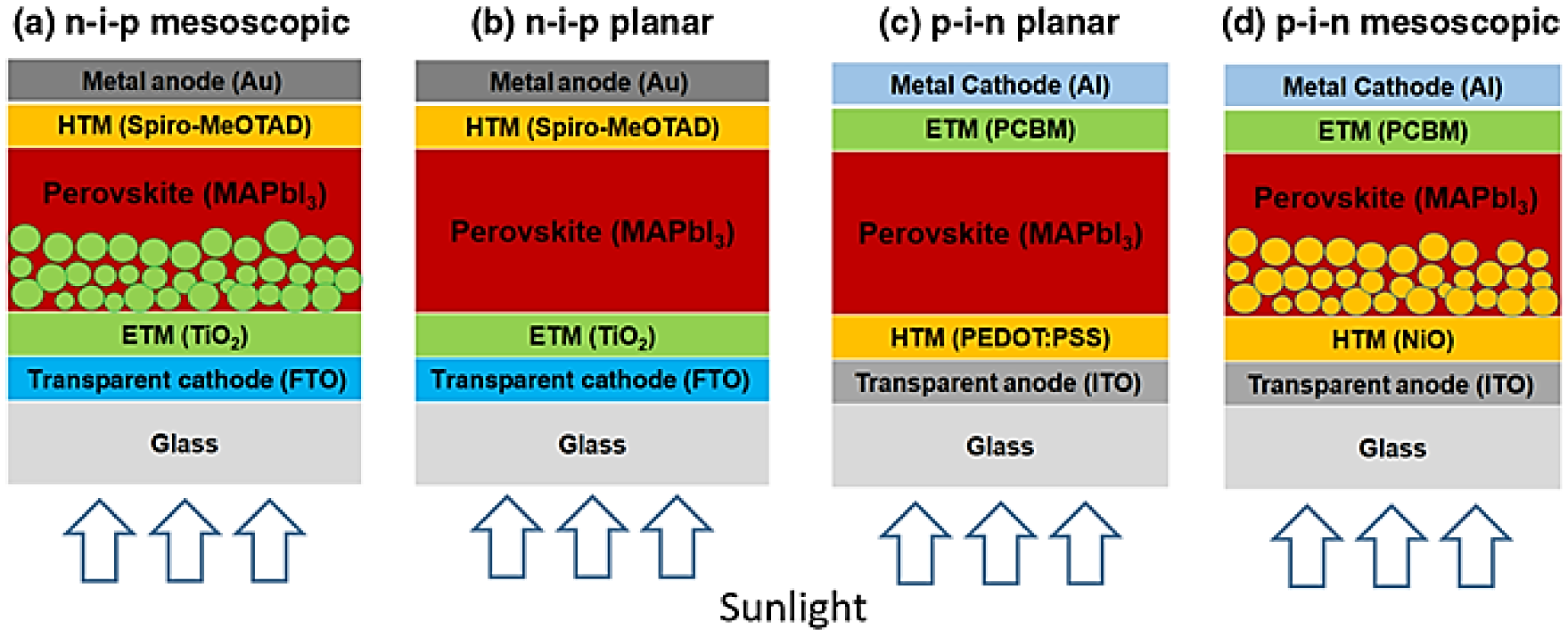
Figure 1. Schematic illustration of different PSCs [2].
Lead methyl ammonium iodide (CH3NH3) is a good choice for the selection of light absorber materials for solid-state mesoheterogeneous solar cells. As shown in Figure 2, perovskite NPs can be prepared by reacting CH3NH3 with PbI2 and accumulating them on TiO2 sheets, which are finally filled with porous conductors (Spir-MeOTAD). By observing the more detailed surface representation, it finds that the performance data of the device under standard AM-1.5 sunlight is shown in Table 1.
Table 1. The performance of the developed solid-state devices [5].
Name | Performance |
Light current (JSC) | 17 mA/cm2 |
Open-circuit photovoltage C (VOC) | 0.88 V |
Fill factor (FF) | 62% |
Notably, when compared to liquid junction batteries sensitized with (CH3NH3)PBI3, perovskite-based devices display improved stability because of the effective charge carrier movement aided by both electrons and holes within the perovskite structure.
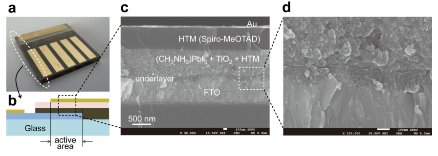
Figure 2. Characterization of the microstructure of solid-state devices [5].
2.1. n-i-p
Common n-i-p structures typically consist of FTO/compact TiO2/perovskite light absorption layer /Spiro-OMeTAD/metal electrode. According to recent reports, the highest efficiency achieved by a formal planar structure [Y: TiO2] as an electron transport material (ETM) in perovskite solar cells is 19.3%. However, these devices exhibit noticeable hysteresis effects.
Formal n-i-p perovskite solar cells employ Spiro-OMeTAD as the hole transport material, which exhibits high photoelectric conversion efficiency but requires doping with various water and oxygen-sensitive ion additives (such as Li salt and Co salt) to enhance its conductivity. Moreover, the presence of acetonitrile solvent used for dissolving Li salt can lead to perovskite degradation, further exacerbating device stability issues. Additionally, it has been observed that biased voltage-induced directional movement of Li+ ions can amplify battery hysteresis phenomena.
2.2. p-i-n
The inverted structure of PSCs exhibits remarkable characteristics. Firstly, the structure consists of five main components: transparent conductive glass, electron transport layer, trans-perovskite film, hole transport layer, and metal electrode. In the inverted configuration, the transparent conductive glass serves as the base rather than the top electrode, enabling light transmission to reach and interact with the trans-perovskite film. The electron transport layer facilitates efficient electron transfer from the trans-perovskite film to the hole transport layer. The trans-perovskite film plays a pivotal role in converting incident light into electricity.
Conversely, in conventional configurations, there is a reversal in position between the electron transport layer and perovskite layer on top of the transparent conductive glass substrate. Furthermore, there is an exchange in functionality between the hole transport layer and electron transport layer within this inverted architecture.
The advantages of employing an inverted structure include simplified and cost-effective fabrication processes that allow for low-temperature deposition techniques without significant hysteresis effects. Moreover, it enables seamless integration with traditional solar cells for constructing tandem devices through lamination approaches. Notably, these inverse structures have achieved impressive photoelectric conversion efficiencies up to 22.7%, highlighting their potential for practical applications. However, the optimization of specific strategies related to the working principle, material selection criteria, preparation methods or performance of reverse-structure perovskite solar cells is still being gradually studied.
3. Interface engineering
Interface engineering is critical to the development of solar cells, and Yin et al. have proposed a viable scheme for enhancing the scalability of solar cells by incorporating multiple two-dimensional (2D) materials in the inner and middle layers of the PSCs [3]. For example, graphene is integrated in dense mesoporous TiO2 and two-dimensional titanium carbide (Ti3C2Tx MXene) is integrated in the absorption layer of perovskite. By employing this strategy, they achieved a 10% improvement in PSC efficiency compared to PSCC without 2D materials. Importantly, they successfully scaled up the optimized structure of 2D materials from laboratory-scale cell sizes to substrates measuring 121 cm2 (11×11 cm2) and 210 cm2 (14.5×14.5 cm2), respectively, resulting in effective area efficiencies of 17.2% and 14.7%. Mesoporous Al2O3 scaffolds can be used to enhance the PCE to 10.9% by minimizing energy losses, demonstrating an effective approach for PCE improvement. In a similar vein, Etgar et al. explored the elimination of hole conductors in mesoscale perovskite solar cells, aiming to utilize perovskite as both the absorber and hole conductor [6]. This can increase PCE to 10.9% by reducing energy loss in the battery.
3.1. HTM and perovskite
PCE of the PSCs, addressing the stability issue between hole transport materials (HTM) and perovskite is crucial, which also serves as a primary research focus in HTM-perovskite interface engineering. Initially, poly(3,4-ethylenedioxythiophene)-poly(styrenesulfonate) (PEDOT:PSS) was extensively investigated and utilized due to its favorable thermal stability, high light transmittance, excellent mechanical flexibility, and suitable energy level alignment. Moreover, it facilitates optimized contact between the hole transport layer and perovskite layer while reducing defects and series resistance. However, PEDOT:PSS exhibits poor compatibility with perovskite within the device structure as its acidic nature often triggers reactions with alkaline methylamine present in organometallic trihalide perovskites. Additionally, since perovskite is highly sensitive to moisture ingress, PSS exacerbates battery instability issues owing to its hygroscopic properties [7]. Because of the limitations of PEDOT:PSS, its alternatives are also the focus of research.
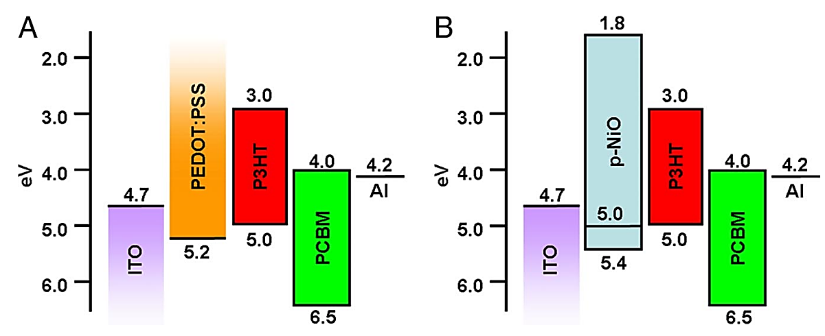
Figure 3. Energy level diagram of equipment components [8].
The PEDOT:PSS layer is a component of a polymerized object heterojunction (BHJ) solar cell, and Irwin et al initially proposed substituting it with a thin P-type semiconductor nickel oxide (NiO) layer to enhance the device’s performance, as shown in Figure 3. Will the incorporation of a thin p-type oxide semiconductor NiO layer (5-80 nm) in the ITO/NiO/P3HT:PCBM/LiF/AlP3HT:PCBM structure enable its activation within the organic poly(3-hexylthiophene) (P3HT)+phenyl-[6,6]-c61 butyric acid methyl ester (PCBM) interface on the ITO anode. The interfacial NiO layer was directly deposited onto cleaned ITO using pulsed laser deposition, followed by spin coating of the active layer. This combination of NiO layers aims to minimize interface losses, thereby improving battery efficiency and filling factor. Consequently, an impressive 5.2% efficiency level was achieved [8].
4. Spraying technology
Flexible PSCs can be created by ultrasonically spraying TiO2 nanoparticles onto polymer substrates. Precursor solutions with various concentrations of TiO2 nanoparticles (0.5 mg/mL, 1.0 mg/mL, and 2.0 mg/mL) were made by dispersing them in ethanol. These solutions were subsequently sprayed onto conductive substrates to create dense TiO2 films of varying thicknesses (from 30 nm to 150 nm). The power conversion efficiency (PCE) of the PSC device was 14.32% after diisopropanol (acetylacetone) titanium (TAA) was added to TiO2-ethanol solution at a molar ratio of 1.0mol% in relation to the TiO2 content to further enhance the film quality. Additionally, 10.87% of both the indium-doped tin oxide coated flexible substrate made of polyethylene naphthalene difluoride (ITO-PEN) and ITO-glass were coated with TiO2.
Ultrasonic spraying technology is a process that utilizes ultrasonic vibration to atomize liquid coating by converting electrical energy into high-frequency mechanical energy through the piezoelectric effect. The resulting atomized particles are then uniformly sprayed onto the substrate surface, offering advantages such as gentle and uniform atomization, non-clogging spray gun, and highly controllable spray flow.
4.1. Nozzle
The atomization effect is primarily influenced by the nozzle structure and ultrasonic wave frequency. Generally, a simpler nozzle structure leads to better atomization due to reduced liquid flow resistance and droplet polymerization caused by complex structures. Increasing the ultrasonic wave frequency results in finer atomized particles and improved atomization effect, albeit at lower power levels. Therefore, it is essential to select an appropriate nozzle design and frequency based on specific applications.
4.2. Sauter mean diameter
The Sauter’s mean diameter (SMD) is defined as the ratio of the total surface area required to the total volume required, serving as a measure of droplet size distribution. Decreasing SMD enhances both contact area between liquid and environment and overall droplet surface area, thereby improving atomization efficiency. Figure 4 illustrates SMD distributions at 0.6 MPa hydraulic pressure for various coaxial and radial distances denoted as A and b [10]. At an axial distance of 240mm, airless nozzle achieves optimal atomization effect with a spray pattern that initially decreases before increasing again due to continuous fragmentation of droplets within this range. As axial distance increases from 240mm to 440 mm, smaller droplets in the spray collide and coalesce, resulting in increased volume. When air pressure is set at 0.2 MPa, inner mixing nozzle exhibits superior atomization performance at an axial distance of 240 mm while outer mixing nozzle performs best at 340mm. Notably, both air-assisted and airless nozzles exhibit similar trends in SMD changes during this process. These findings suggest that longer external nozzles can yield improved atomization results by facilitating enhanced dispersion characteristics. Furthermore, when compressed air pressure reaches 0.4Mpa, patch density variation is relatively minor for outer mixing type compared to inner mixing type due to structural features enhancing spray coverage [9].
The Sauter mean diameter (SMD) of airless and internal mixing nozzles exhibits a negative correlation with the radial distance, resulting in maximum values at the spray center. In contrast, the SMD of outer mixing nozzles shows a positive correlation with the radial distance. The action of outer mixing nozzles causes fragmentation of droplets at the spray center, preventing their enlargement due to collision effects. As shown in Figure 4, at equivalent radial distances, airless nozzles exhibit larger SMDs, indicating that compressed air is an effective means to enhance atomization across different radial distances. Additionally, when compressed air pressure is held constant, the SMD of outer mixing nozzles significantly exceeds that of inner mixing nozzles [10-12].
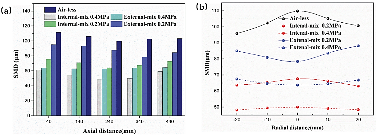
Figure 4. SMD distribution at different axial distance and radial distance [9].
5. Conclusion
Interface engineering and ultrasonic spraying technology are important directions for the development of perovskite solar cells, which can provide an effective way to improve the efficiency and stability of the cell. However, there are still some challenges and problems in interface engineering, such as the selection and optimization of modifiers, the thickness and uniformity control of intermediate and protective layers, and the complex reaction mechanism at the interface. Therefore, it is necessary to further study the basic principles and action mechanisms of interface engineering, and develop more efficient, stable and environmentally friendly interface materials and methods. In addition, the theory and mechanism of ultrasonic spraying technology still need to be further studied, because ultrasonic atomization is a complex nonlinear dynamic process, involving liquid surface tension, viscosity, density, surfactant, gas pressure, temperature and other factors, there is no unified mathematical model and physical interpretation to describe and predict its behaviour.