

1. Introduction
RISC-V is an instruction set architecture (ISA) that is open and free. It has generated a lot of interest in the field of computer science due to the fact that it has the potential to completely transform the way that processors and systems are designed [1]. RISC-V has a wide range of applications thanks to its versatility and flexibility. These applications include low-power embedded devices, high-performance computation, computer security, and machine learning [1-3]. It is likely that RISC-V's influence on the global chip industry, as well as the wider technological environment, will increase as it continues to flourish [3]. This heralds a future that is both innovative and exciting.
This paper uses Verilog hardware description language to design a five-stage pipeline CPU. Using the Vivado 2022.2 simulation software, the CPU is designed to support RV32I 37 basic instructions and a multiplication extension instruction. The ALU module is optimised with carry look-ahead adders, barrel shifters and multipliers combined with the Wallace tree booth algorithm. Create a test file to run a mock test, then check the waveform it generates to see if it executes the instructions correctly. In addition, synthesise generates RTL diagrams, judges whether the design structure requirements are met, and analyses resource occupancy according to the synthesised report. The CPU has guiding significance for the processor design of embedded and Internet of Things devices and also provides a new design idea for the optimization of the pipeline and ALU in the processor.
2. Basic theory of RISC-V and its development prospect
RISC-V refers to the fifth generation of reduced instruction set. The primary advantage of RISC-V is its adaptability and customisation. The architecture is organised as a modest ISA foundation with several optional extensions. This design methodology enables developers to customise RISC-V processors to meet the specific needs of their applications, making them appropriate for a wide range of computing devices. The European Processor Initiative has adopted RISC-V for designing and manufacturing supercomputing CPUs [2].
The pervasive adoption of RISC-V across many domains demonstrates its versatility. RISC-V has demonstrated its ability to operate a variety of embedded systems, from consumer devices and Internet of Things (IoT) devices to automotive, industrial, and medical applications. In addition, the telecommunications and mobile industries, as well as peripheral computing and data centres, have embraced RISC-V [3]. As a consequence, RISC-V has become a crucial component in the advancement of technology across multiple industries.
Growing interest in RISC-V extends to computer security research, where hardware- and architecture-based security techniques are being investigated. Tao Lu's comprehensive survey extensively explores the security aspects of the RISC-V architecture, covering various key areas, including hardware and physical access security, etc. [1]. This demonstrates the capability of RISC-V to address security issues and bolsters its importance in the field of cybersecurity.
Machine learning is another area where RISC-V is acquiring momentum. Researchers have provided a quantitative taxonomy of RISC-V Systems-on-Chip (SoCs) and identified future machine learning research opportunities using RISC-V open-source hardware designs [1]. The open nature of RISC-V enables the construction of specialised hardware accelerators to improve the performance of machine learning. This creates new opportunities for RISC-V substantially contributing to the growth of machine learning technologies.
RISC-V's continual development and research indicate a bright future for the ISA. The fact that it is accessible and free to use fosters a thriving ecosystem of research and development, resulting in continuous enhancements and innovations. Recent research indicates that RISC-V has the potential to remain at the vanguard of advances in computer science and the chip industry.
3. Design and implementation
3.1. instruction set selection
First, determine the instruction set to be implemented. To implement 37 instructions in RV32I and an extended multiplication instruction shown in table. 1.
Table 1. Chosen instruction [4].
Instruction Category | Example Instructions | Description |
R-Type I-Type U-Type J-Type B-Type S-Type | add, sub, sll, slt, sltu, xor, srl, sra, or, and, mul addi, slti, sltiu, ori, xori, andi, slli, srli, srai lui, auipc jal, jalr beq, bne, blt, bltu, bge, bgeu sw, sh, sb lw, lh, lb, lhu, lbu | Performs arithmetic and logical operations on two registers and stores the result in rd. Performs arithmetic and logical operations on a register (rs1) and an immediate value and stores the result in rd. Loads a value into the highest 20 bits of a register (lui) or adds a value to the PC (auipc). Performs an unconditional jump (jal) or jump register (jalr) to a target address specified by an immediate or register value. Performs conditional branches based on the comparison of two registers with an immediate value. Loads or stores register data into memory. Two registers and an instantaneous value calculate the effective address. |
There are six different types of instruction. Then use Verilog to develop and design a single-cycle CPU that can execute the above instructions in Vivado 2022.2 [4, 5]. The whole CPU structure was designed as shown in Figure 1.
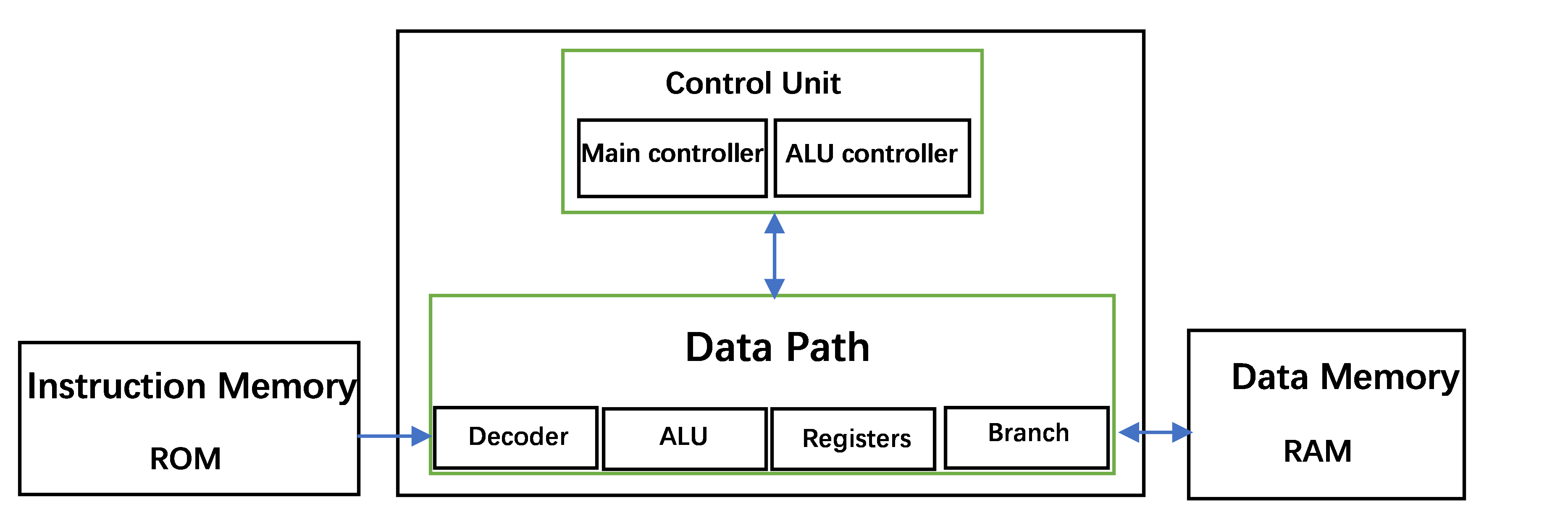
Figure 1. CPU structure [4].
3.2. Data path
The data path includes four modules: Decoder, ALU, Registers, and Branch [5]. Decoder is responsible for decoding instructions and splitting them into opcode, function code, registers number and immediate counting parts. Then the ALU calculates a result based on the input control signal and the values in RS1 (operating register 1) and RS2 (operating register 2) for output. Registers serve as essential modules within the CPU, responsible for storing both data and addresses. In the RISC-V fundamental ISA, there are 31 general-purpose registers specifically designed for holding integer values. Notably, Register x0 is unique, as it always holds a constant value of 0 [5]. These registers play a crucial role in facilitating efficient data manipulation and computation within the CPU, contributing to the overall performance and functionality of the RISC-V architecture. A program counter (PC) register is also accessible to the user and stores the address of the current instruction. The branch is the part of the CPU responsible for implementing conditional jumps. It judges whether the branch condition is satisfied according to the condition code (funct3) of the instruction and the value of two registers (rs1 and rs2). According to the instruction's immediate value, it determines the destination address. Whenever the branch condition is satisfied, write the target address to PC; otherwise, add 4 to PC and continue to execute the next instruction.
3.3. Control unit
The control unit includes two modules, Main control and ALU control, which are the components in the CPU responsible for generating control signals. It determines the type, format and function of the instruction according to the operation code (opcode) and function code (funct3 and funct7) of the instruction. It generates corresponding control signals to control the work of other components.
3.4. 5-Stages flow
The processor's instruction execution is carried out through a well-structured five-stage pipeline: fetching, decoding, executing, accessing memory, and writing back [6, 7]. This architectural approach effectively divides the execution process into smaller, more manageable stages, akin to breaking down a large combinational logic into five smaller combinational logics. Each of these smaller modules is designed to be executed within a single cycle, resulting in a notable reduction in the CPU clock cycle and the potential for increased CPU frequency.
Implementing the pipeline requires more than just reorganizing and packaging modules; it involves a meticulous interruption of the "path" between each submodule. Despite the interruption, the original signal circulation between the submodules must remain unaltered. To achieve this, a set of pipeline registers is introduced between the two submodules, ensuring seamless data flow and synchronization throughout the pipeline stages. This clever design approach optimizes the CPU's performance, enabling it to execute instructions efficiently and enhance overall processing speed.
3.5. Optimisation of the ALU
The last is the optimization of the ALU module. The addition is the fundamental mathematical operation and an essential ALU operation. Addition logic includes ripple adder, carry choose adder, and others. These circuits have extensive propagation delays because the carry-sum of higher bits depends on the carry-out of lower important bits. CLA resolves this issue. Inputs calculate each bit's carry-sum with this method [8].
Theoretically, when designing a 32-bit CLA adder, all carry, and standard bits can be generated in parallel at the same time, but this will make the circuit structure very complicated and greatly increase the fan-in and fan-out of the circuit, which is not feasible in actual design. Therefore, a 32-bit adder is implemented in parallel within a group and between groups; that is, a 4-bit CLA adder is implemented first, and then a 16-bit CLA adder is implemented in parallel between groups of four 4-bit CLA adders, and a 32-bit CLA adder is implemented in parallel between groups of two 16-bit CLA adders as figure 2 shown. This design scheme takes advantage of the low delay of CLA, shortens the longest calculation path, and avoids making the circuit too complicated. It is an ideal 32-bit adder design scheme.
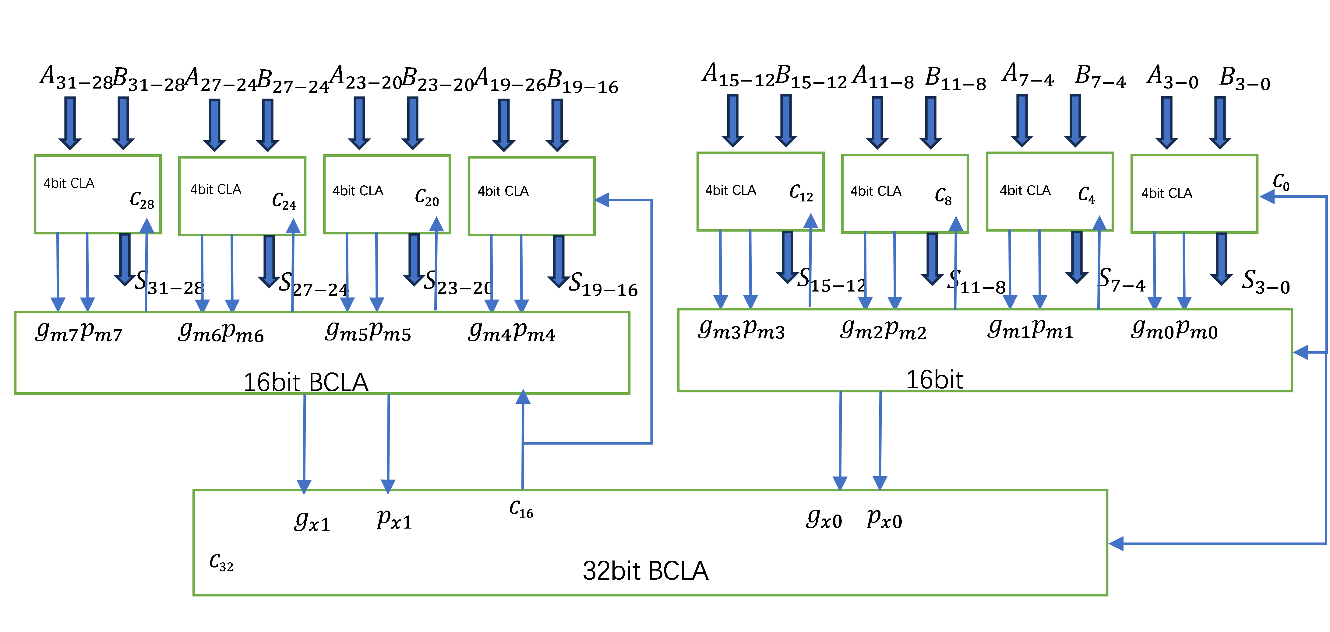
Figure 2. CLA adder [8].
A barrel shifter that can rotate or shift a data word by any number of bits in a single clock cycle. It connects the input data word directly to the correct position of the output without cascading shifts over multiple clock cycles. This increases the speed of the shifter and reduces latency [9]. The barrel shifter can also realise different shift or rotation functions according to the control signal, such as logical left shift, arithmetic right shift, etc., which can meet the needs of the CPU and reduce time delay. The integration of multiple shift functions also makes it highly versatile.
The multiplier is jointly optimised through the booth algorithm combined with the Wallace tree and the CLA designed earlier to reduce the time delay. The Booth algorithm is a multiplication algorithm using two's complement, which reduces the number of partial products, thereby reducing the complexity and delay of the multiplier [10]. Wallace tree: A multiplier structure that uses a compressor, Wallace trees are able to split the addition of partial products into numerous levels and utilise compressors at each level to concurrently lower the number of bits in each partial product. Wallace trees are an efficient way to decrease the multiplier's size and power requirements while increasing its speed. Figure 3 illustrates the construction of the whole Wallace tree structure utilising multiple 3-2 compressors and a 4-2 compressor reduction.
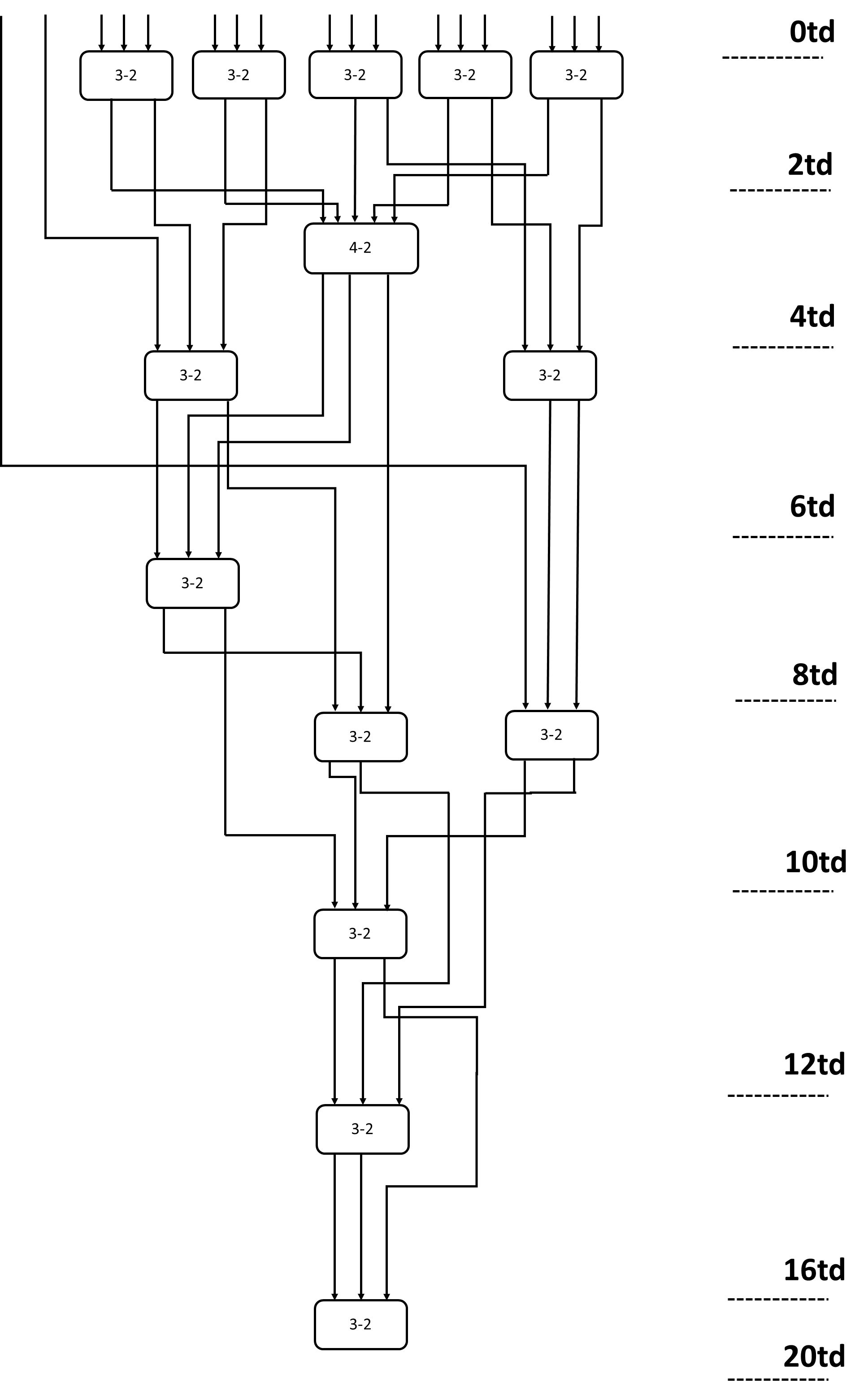
Figure 3. Wallace tree [10].
4. Simulation verification
Ripes is an open-source RISC-V CPU simulation software, which can convert the written assembly language into the corresponding machine code and can run instructions and view the data in registers or memory in real time. Vivado is a well-known development and simulation test tool that plays a key role in the CPU design process. Its powerful capabilities include compilation, synthesis, and implementation of hardware Verilog descriptions; during synthesis, Vivado efficiently configures various logic resources, including look-up tables, flip-flops, and RAM, and strategically arranges them within the FPGA to create well-structured circuits. This complex arrangement ensures the seamless integration of different functions and enables our complex CPU design. First, use the open-source tool Ripes to convert the selected assembly instructions into the machine code required for the test, and then write the test file in Vivado to generate the waveform diagram and synthesise the circuit and report.
4.1. instruction verification
As shown in Figure 4, write a program that adds -0xff, 4, and 0xff to the value in the r0 register and stores them in r1, r2, and r3, and then logically shifts the value in R1 to the left. Logical right shift and arithmetic right shift are written back to the R4, R5, and R6 registers, respectively.
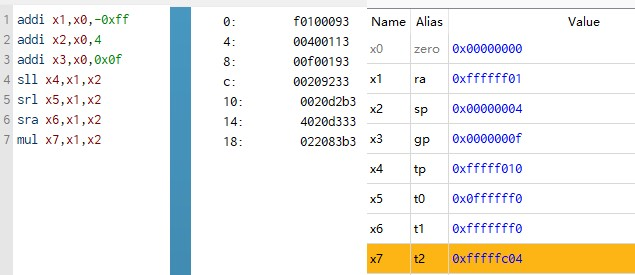
Figure 4. Instructions in Ripes (Photo/Picture credit: Original).
As can be seen from Figure 5, the adder and shifter can work normally and write the correct value into the corresponding register. Finally, verify the multiplication, and multiply the value in R1 and R2 to get the correct result 0xfffffc04.
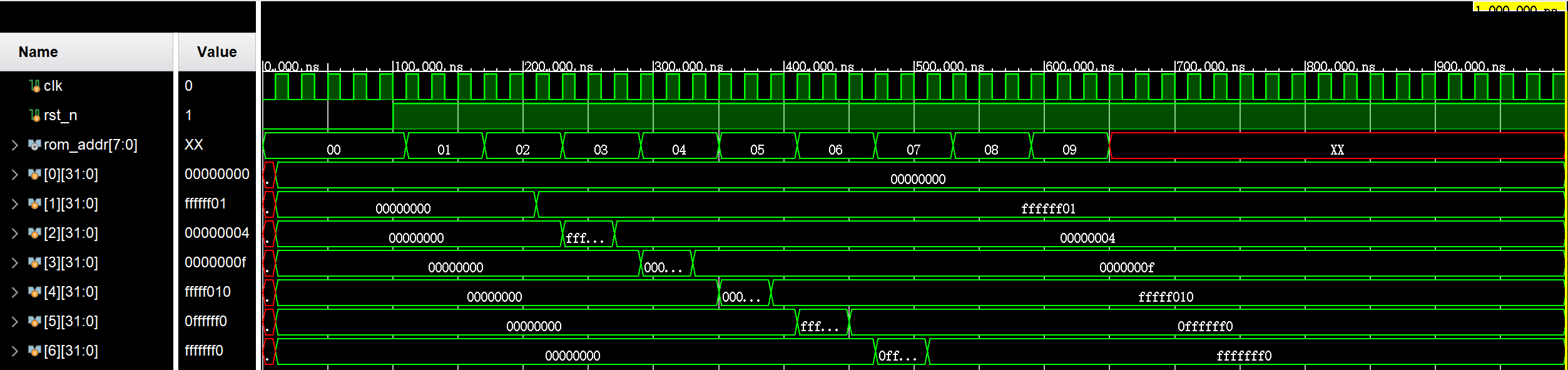
Figure 5. Waveform (Photo/Picture credit: Original).
4.2. Synthesise and resource occupation analysis
Use Vivado to synthesise the code and generate the RTL graph of the CPU, as Figure 6 shown. You can see that the generated synthesis graph includes instr_memory (instruction memory), control_inst (control unit) and datapath_inst (Datapath) three parts. It can also be seen that the output (PC value) of the top-level module is on the right.
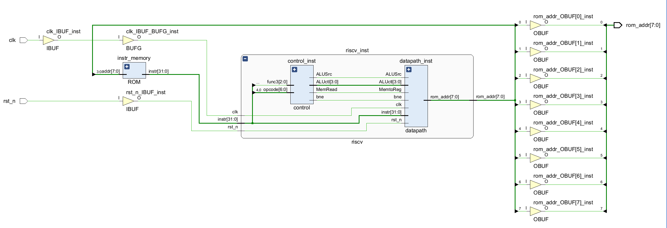
Figure 6. The RTL graph of the CPU (Photo/Picture credit: Original).
From the project report in Vivado, the data in Table. 2 can be accessed. It can be noticed that the barrel shifter saves the occupation of LUT resources due to its structural design. The abbreviation "LUT" stands for "Look-Up Table." A Look-Up Table is a data structure or a hardware component that, in the context of computer science and digital logic, is used to execute logic functions or mathematical operations in a way that is computationally efficient. This can be accomplished in a number of different ways. Lt is an essential resource in FPGA.
Table 2. Resource usage comparison.
Normal shifter | Barrel shifter | |
LUT IO | 204 71 | 185 71 |
5. Conclusion
The designed pipeline CPU structure meets expectations. it executes instructions accurately and produces expected results after ALU optimisation. The waveforms clearly correspond to register values in Ripes, confirming proper CPU functionality. It successfully performs basic operations such as addition, shift, and multiplication, demonstrating its versatility and computational power. Moreover, the perfect execution cycle of the five stages of an instruction confirms the successful implementation of the five-stage pipeline, which greatly enhances the performance and throughput of the CPU. A comprehensive report analysis shows that the optimised barrel shifter effectively utilises 19 LUTs compared to conventional shifters, which represents a significant saving of circuit resources.
Looking ahead, there are many opportunities for further improvement and expansion. Additional designs can be incorporated into decode and control blocks, enabling the CPU to support a wider range of instructions, enhancing its versatility and capabilities. Exploring innovative approaches, such as combining shifters and adders, can further optimise multiplier structures, helping to improve circuit resource efficiency. The successful development of this pipelined CPU lays a solid foundation for future endeavours. Building on this achievement, it is also possible to create a complete SoC based on this CPU to meet the needs of various computer systems and microprocessors. This holistic approach promises to deliver enhanced performance and simplified integration, making CPU a compelling choice for a wide variety of computing applications.