


1. Introduction
According to the Heart Disease and Stroke Statistics published by the American Heart Association (AHA), in 2020 alone, there were about 19.5 million deaths worldwide due to cardiovascular disease (CVD), and CVD is therefore listed as one of the leading causes of death [1]. The monitoring and scientific treatment of cardiovascular signals can effectively prevent the deterioration and death of cardiovascular diseases. Electrocardiogram has been used in clinical medicine for hundreds of years, and with the development of electronic technology, portable wearable electrocardiograph has appeared [2]. Compared with the 12-lead Electrocardiograph (ECG) used in clinical practice [3], wearable ECG devices generally have only two or three electrodes, that is, one lead [4]. Although the captured signal is not enough for accurate medical diagnosis, it can effectively capture sudden and unpredictable disease signals by monitoring ECG signals for a long time. In practical application, the use of networking equipment can achieve real-time monitoring of the patient's heart health status. It also effectively preventing the disease cannot be found in time, so the delay of gold rescue time.
Practical application scenario, due to the ECG signal being weak, amplitude between 0.4 and 2.5 mV, and frequency limit between 0.1 Hz - 150 Hz. After taking ECG of children into account, it even need to raise the upper limit of frequency response to 250 Hz [5]. At the same time, ECG signals are susceptible to interference from flicker noise, thermal noise, white Gaussian noise and 50Hz(China, etc.)/60Hz(the United States, etc.) noise [6]. Therefore, the wearable ECG device is required to have a good common mode rejection ratio (CMRR), which can effectively amplify useful signals and suppress noise. To make the device have a stronger battery life, there are also strict requirements for power consumption. The size of the device must be considered throughout the design phase as well, and it is not appropriate to use large capacitors. In view of the above requirements, a second-order and 3-op amp circuit based on an instrumentation amplifier was designed by referring to a low-power and low-noise Complementary Metal-Oxide-Semiconductor amplifier for neural recording applications jointly proposed by Harrison and Charles [7]. To solve the problem of the unknown common-mode input level of the circuit, a right-leg driving circuit model is introduced between the first-order circuit and the first-order circuit. The common-mode feedback is used to reduce its interference [8], so that the body voltage falls within the common-mode input range of the amplifier.
This paper focuses on the theoretical circuit module design, LTSPICE simulation and data analysis.
2. Method
2.1. Application requirements analysis
According to the requirements of practical application scenarios, this paper designed a wearable device with low noise (total integrated input-referred noise < 4 μV), low power consumption (total power consumption of all blocks < 5 μW) and small size (total amount of employed capacitance < 1 nF) that can meet the amplification of 0.1 Hz - 250 Hz signals (differential mode gain = 40 dB) through theoretical analysis, and simulate the design circuit through LTSPICE to verify its performance.
2.2. Experimental theoretical model
2.2.1. Classic 3-op-amp instrumentation amplifier. As shown in Figure 1, compared with the first-order OP amp circuit constructed by a single operational transconductance amplifier, the second-order 3- operational amplifier (op-amp) circuit adds a fully differential input buffer before differential to a signal-ended amplifier whose common mode gain is equal to 1. Therefore, the first-order circuit module just only amplify the useful difference mode signal, and not amplify the common mode signal. It can effectively improve the CMRR and increase the anti-interference ability of the circuit to the common mode noise.
The differential mode gain of the first-order circuit is given by equation (1):
\( {A_{v1,dm}}=1+\frac{{R_{f1}}+{R_{f2}}}{{R_{g}}}\ \ \ (1) \)
The common mode gain of the first-order circuit is given by equation (2):
\( {A_{v1,cm}}=1\ \ \ (2) \)
The differential mode gain of the second-order circuit is given by equation (3):
\( {A_{v2,dm}}=-\frac{{R_{2}}}{2{R_{1}}}-\frac{{R_{4}}({R_{1}}+{R_{2}})}{2{R_{1}}({R_{3}}+{R_{4}})}\ \ \ (3) \)
The common mode gain of the second-order circuit is given by equation (4):
\( {A_{v2,cm}}=-\frac{{R_{2}}}{{R_{1}}}+\frac{{R_{4}}({R_{1}}+{R_{2}})}{{R_{1}}({R_{3}}+{R_{4}})}\ \ \ (4) \)

Figure 1. 3-op-amp instrumentation amplifier.
2.2.2. Operational transconductance amplifier model. To reduce the loss at the input before reaching the amplifier, the partial voltage on the electrode should be as small as possible. Therefore, the designed op-amp is required to have a sufficiently high input impedance. This circuit uses an instrumentation amplifier with a high input impedance, as shown in Figure 2. At the same time, the amplifier should have better noise performance. To reduce the noise, the device size can be increased, that is, the W and L of the metal-oxide-semiconductor field-effect transistor can be increased. The larger the WL of the device, the smaller the flicker noise, but too much WL can affect the capacitive coupling. At the same time, it can also reduce the noise by increasing the current I, but it can cause an increase in power consumption, which needs to make a trade-off in the design process.

Figure 2. OTA internal structure.
2.2.3. Driven-right-leg circuit. During the bioelectric potential measurement, the collected data are easily affected by electromagnetic interference, and the introduction of the driven-right-leg circuit can effectively reduce the common mode interference [8]. Without the driven-right-leg circuit, there is only a 3-op-amp instrumentation amplifier in the circuit, which causes a problem: the body voltage magnitude, that is, the common mode input level is unknown. The driven-right-leg circuit, as shown in Figure 3, essentially adds a common mode extraction circuit. It can extract the reference voltage through the Auxiliary op amplifier, and then return the resulting Vcm to the body electrode. This Vcm signal can effectively cancel the common mode signal. After introducing the driven-right-leg circuit, there is no need to use resistance feedback to the op-amp to set the bias voltage, this work is done by the driven-right-leg circuit. At the same time, the circuit has the following advantages: the input common mode of the instrument amplifier can be set by feedback, and the common mode pickup noise can be reduced. At the same time, the circuit enables a safe way to ground the body, especially with current limiting resistor Ro. If the body voltage increases abnormally, the op amp can enter the saturation region. Effectively unground the body pole in the circuit.

Figure 3. Driven-right-leg circuit.
2.2.4. Human-body circuit model. The acquisition of ECG signal amplitude is small and vulnerable to a variety of noise interference. Thus, it is very necessary to build a human-body electrode model to simulate the signal collection, as shown in Figure 4. Among them, the current source simulates the low-frequency noise of the human body at 60 Hz, and the resistance of 200 Ω is used to simulate the resistance between the two ends of the human body.

Figure 4. Human body circuit model.
3. Results
3.1. Circuit design
Through the integration and analysis of the above theoretical model, an ECG sensor amplification circuit based on a secondary operational transconductance amplifier (OTA) model op amp is designed, as shown in Figure 5. The simulation is carried out through LTSPICE to verify the operating characteristics of the circuit.

Figure 5. Low power wearable ECG sensor circuit model based on secondary OTA.
3.2. Data analysis
3.2.1. Gain and bandwidth.
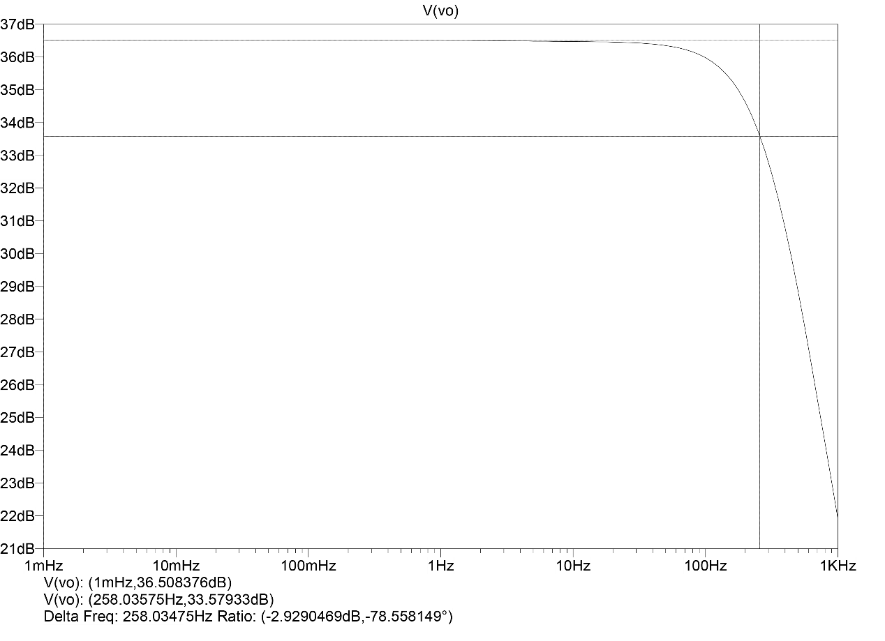
Figure 6. AC analysis.
In circuit design, the first-order circuit mainly starts from the amplification circuit. According to formula (1), the designed theoretical difference mode gain is as follows:
\( |{A_{v1,dm}}|=20{log_{10}}{|1+\frac{500k+500k}{10k}|}=20{log_{10}}{1}01≈40dB\ \ \ (5) \)
econd-order circuit mainly plays a filtering role, which can be obtained from equation (3), and its theoretical difference mode gain is as follows:
\( |{A_{v2,dm}}|=20{log_{10}}{|-\frac{6.36M}{2×6.36M}-\frac{6.36M×(6.36M+6.36M)}{2×6.36M×(6.36M+6.36M)}|}=20{log_{10}}{1}=0dB\ \ \ (6) \)
heoretical cut-off frequency is:
\( {f_{c}}=\frac{1}{2πRC}=\frac{1}{2×π×6.36M×100p}≈250Hz\ \ \ (7) \)
In LTSPICE, the gain and bandwidth of the circuit are obtained by performing a 1 mHz-1 kHz AC scan on the circuit. As shown in figure 6 it is not difficult to see the total differential mode of the circuit gain of 36.5 dB, cutoff frequency (-3 dB frequency) approximately 250 Hz. The difference of 3.5 dB between the measured value of difference mode gain and the theoretical value is caused by the loss caused by the human-body electrode model, and the measured value of bandwidth is consistent with the theoretically calculated value.
3.2.2. Noise analysis. As shown in Figure 7, the total integrated output-referred noise can be obtained by noise analysis in LTSPICE. To measure the figure, the total integrated output-referred noise is 263.83 μV. To get the total integrated input-referred noise, simply divide the total integrated output-referred noise by the linear value of the gain. The calculated total integrated input-referred noise of the circuit is 3.94 μV, which meets the design requirements, that is, the input-referred noise is less than 4 μV.
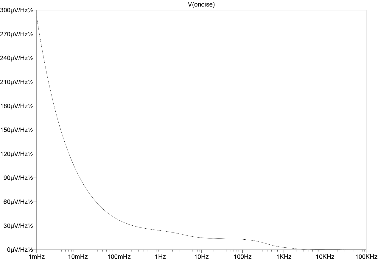
Figure 7. Noise analysis.
3.2.3. Power consumption. Most of the power of the circuit is dissipated on the OTA. In the design process, to lower the circuit's power consumption, there are two options to choose from. The first one is to lower the voltage of the power supply, and the other is to reduce the bias current of the current source. At the same time, it also increases the noise to a certain extent, so it needs to balance and choose. In this circuit, the OTA driving voltage used is constant 1.8 V, so the second method is used here, that is, to reduce the bias current to reduce the power consumption. After the simulation of the circuit, the power consumption of the circuit is measured to be 4.67 μW, which meets the design requirements, that is, the total power consumption is < 5 μW.
3.2.4. Common mode rejection ratio. In the previous AC scan, the difference mode gain of the circuit was 66.83, that is, 36.5 dB. By measuring the common mode gain can obtain the value 0.021, that is -31 dB. Therefore, by dividing the differential mode gain by the common mode gain's linear value, the CMRR may be calculated. The value is 3182, which is equal to 70 dB.
3.2.5. Noise efficiency factor. The calculation formula of the Noise efficiency factor (NEF) is given by equation (8):
\( NEF={V_{n,in,RMS}}{(\frac{{I_{tot}}}{{ϕ_{t}}\cdot 4kT\cdot BW\cdot \frac{π}{2}})^{\frac{1}{2}}}\ \ \ (8) \)
In formular, \( {V_{n,in,RMS}} \) means the sum of the input-referred noise. \( {I_{tot}} \) means total amplifier current (including all OTAs and all branches). \( {ϕ_{t}} \) means thermal voltage. K is the Boltzmann constant. T is the temperature in Fahrenheit. BW is the bandwidth of the circuit. The NEF of the circuit can be calculated by equation (8):
\( NEF=3.94μ×{(\frac{2.6μ}{25m×4×1.38×{10^{-23}}×298×250×\frac{π}{2}})^{\frac{1}{2}}}=15.8\ \ \ (9) \)
4. Discussion
Through LTSPICE simulation, it can be seen that this design meets the design requirements proposed at the beginning of the article, that is, achieves the requirements of low power consumption and low noise. In general, the ECG's signal frequency is between 0.05 Hz and 150 Hz, and the bandwidth of this circuit is appropriately widened to 250 Hz to make it suitable for the ECG frequency range in the pediatric examination. The larger bandwidth means more noise, which also brings a greater challenge for low-noise circuit design. At the same time, this circuit can effectively capture the ECG signal and amplification. Compared with Table 1, it can be seen that the lower power consumption enables it to have stronger battery life in the wearable application scenario.
Table 1. Performance Comparison.
[9] | [10] | [11] | This work | |
Bandwidth [Hz] | 0.52-108.6 | 0.2-200 | 0.5-80 | 0-250 |
Gain [dB] | 53.9-59.8 | 35.7 | 60.68 | 36.5 |
Noise [μV] | 3.5 | 4.8 | 27 | 3.94 |
Power consumption [μW] | 70 | 168.82 | NA | 4.67 |
CMRR [dB] | 118.5 | 142.1 | 91.73 | 70 |
This work also has certain limitations. Table 1 shows that, the CMRR of this circuit is 70dB, which is lower than the previous research, and further improvement is possible. Moreover, the OTA size was not accurately calculated during the circuit design. At the same time, the circuit is only simulated in LTSPICE simulation software. The performance of the circuit is not measured in the real environment of the laboratory. In future designs, the CMRR can be improved by improving the circuit structure or adjusting the circuit elements. The gain can be further increased according to the design requirements. If conditions permit, the actual circuit can be made in the laboratory for performance testing.
5. Conclusion
Based on theoretical analysis and LTSPICE simulation, this paper presents the circuit research of low power devices for wearable ECG. Compared with the 12-lead ECG device used in clinical practice, this circuit was designed to address the "low power consumption" of the wearable ECG device. The circuit is mainly composed of three modules. The first-order circuit for fully differential input buffer, was used for amplification ECG signals were collected (i.e., differential mode signal). The second-order circuit is a differential to signal-ended amplifier, which can play the role of filtering and limit the circuit bandwidth to the range of 0-259 Hz. The driven-right-leg circuit is introduced between the first and second-order circuits to set the bias voltage and protect the human body at the same time. The design process was from theoretical model analysis to LTSPICE simulation. The simulation performance was consistent with the theoretical design after considering the human body electrode model (which brings 3.5dB attenuation). Because the wearable ECG device should meet the application needs of long-term wearing, the device size limit is only three electrodes. This prevents it from being used for more demanding medical diagnostic testing, as is the case with the 12-lead ECG, which has 10 electrodes as inputs. However, it provides convenience for monitoring the ECG signal of the wearer in daily life, so that people can detect sudden abnormal ECG signals. In future research, through the design of the electronic system, the circuit can be combined with a Bluetooth module, WIFI module, control module and other functional circuits to broaden the function of the circuit. If it is combined with the mobile application, doctors and family members can observe the physical condition of patients at any time, which can effectively avoid the delay of the disease caused by the failure to find it in time and benefit patients with cardiovascular disease.