


1. Introduction
Today’s MOSFET has been designed into nanoscale. A small chip may include millions of MOSFETs. Back in the day, when the MOSFET was invented, it is pretty large, and its functionality is not as good as today. The engineers have developed MOSFETs for decades and optimized their size, power consumption, and other performance. Therefore, modern MOSFET technology has made significant advancements. High-performance MOSFETs now offer improved power handling capabilities and reduced heat generation. New materials and designs enable faster switching speeds, enhancing efficiency in high-frequency circuits. Advanced MOSFETs also feature lower on-resistance, enabling higher current flow, and innovations like silicon carbide (SiC) and gallium nitride (GaN) MOSFETs offer superior performance in high-voltage and high-power applications. Despite the progress made in modern MOSFET technology, several limitations still exist. One major concern is the increasing demand for power density and miniaturization, which leads to challenges in heat dissipation and reliability. As MOSFETs continue to shrink in size, issues like leakage current and quantum effects become more pronounced, affecting overall performance and energy efficiency. To address these limitations, future advancements should focus on developing innovative materials, such as 2D materials or wide-bandgap semiconductors, to improve power handling and reduce leakage. Moreover, optimizing the design and architecture of MOSFETs, exploring new gate dielectric materials, and enhancing thermal management techniques will be crucial to unlocking their full potential in next-generation electronics. Therefore, this paper introduces the overall view of modern MOSFETs and how they perform in the circuit. By delving into the unique characteristics and design considerations of nanoscale MOSFETs, this paper aims to shed light on the future prospects and research directions in this rapidly evolving field.
2. History of MOSFET
The concept of MOSFET was proposed by Lilienfeld in 1925, but he was unable to create FET as shown in Figure 1. In 1959, Mohamed Atalla and Dawon Kahng invented the MOSFET at Bell Labs. The first MOSFET has a channel length that is greater than 20 μm. While today’s MOSFETs are under the scale of nanometers. In 1962, Frank Wanlass invented the complementary metal oxide semiconductor (CMOS) [1]. However, CMOS did not dominate integrated circuits until 1981. The main reason is that PMOS does not have a better performance compared to NMOS. For example, if a CMOS inverter is built to have exact propagation delay tPHL and tPLH, the width of PMOS has to be made greater than the width of NMOS [2]. The primary CMOS advantage is low power consumption, which is a key reason in today’s integrated circuit.
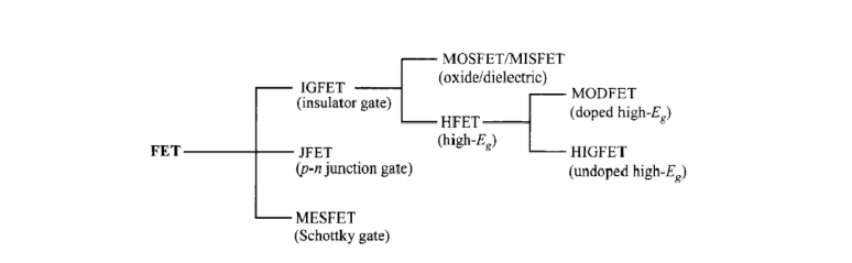
Figure 1. Family tree of field-effect transistors.
However, during the period from 1920s to 1980s, MOSFETs were not commonly used. Instead, this era witnessed the dominance of vacuum tubes and early bipolar transistors. Vacuum tubes, such as triodes and pentodes, were extensively utilized in electronic devices like radios, televisions, and early computers. It wasn’t until the late 1960s that MOSFETs started to gain attention. Their primary application during this time was in integrated circuits and digital logic circuits. MOSFETs offered advantages over vacuum tubes and bipolar transistors, such as smaller size, lower power consumption, and increased reliability. Their ability to operate at low voltage levels made them ideal for early microprocessors and memory chips. By the late 1970s and early 1980s, MOSFETs became the preferred choice for digital integrated circuits, leading to the revolution of microelectronics. They facilitated the development of smaller, faster, and more power-efficient electronic devices, paving the way for the modern era of computing, communication, and consumer electronics. Overall, the use of MOSFETs in the old timeframe, as shown in the Figure 2, was primarily focused on the emergence and growth of digital integrated circuits, setting the stage for their widespread adoption in the years to come.
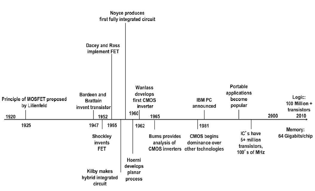
Figure 2. Brief history of CMOS.
After years of technological advancements, during the 1980s, IBM became the pioneer which proposed to let computers help to design ICs so that companies can invent ICs with less error and higher speed. People call this computer program computer-aided design (CAD). Later, Electronic design automation (EDA) is a term for a category of software products and processes that help to design electronic systems with the aid of computers [3]. Now, everything that helps us design ICs are called EDA tools. Today, one of the most famous EDA tool companies is Cadence.
Thanks to the EDA tool, today’s MOSFET has been invented in nanoscale technology, and millions of transistors are built on finger-nail-sized chips. One of the most powerful chips is Apple’s M1 ultra chip, which is built on a 5-nanometer process with 114 billion transistors.
3. Differences analysis
The most obvious difference between modern MOSFET and the old MOSFET is the size. The old MOSFETs are scaled in micrometers while modern MOSFETs are under nanometers. The reduced size of MOSFET brings a noticeable advantage, which is the power supply. Under Dennardian scaling, the reduced size of MOSFET can proportionally reduce the supply voltage. This will result in low power consumption. Today’s supply voltage for MOSFET is around 1.1V. Besides the comparison of modern MOSFET and the old MOSFET, there are also some interesting comparisons in the transistor family as shown in Table 1. For example, BJT and MOSFET, both of them belong to the transistor family, but MOSFET is voltage-controlled device while BJT is a current-controlled device. Due to the property of BJT, using BJT will consume more energy because there is more leakage current when the switch is on. In addition, the current brings heat so BJT has low thermal stability compared to MOSFET. BJT also has higher junction capacitance, which makes the RC time to be larger. Thus, BJT is not allowed to be implemented under high frequency.
Table 1. BJT, FET and MOSFET comparison.
TERMS | BJT | FET | MOSFET |
Device Type | Current-Controlled | Voltage-Controlled | Voltage-Controlled |
Current Flow | Bipolar | Unipolar | Unipolar |
Terminals | Not Interchangeable | Interchangeable | Interchangeable |
Operational Modes | No Modes | Depletion Mode Only | Both Modes* |
Input Impedance | Low | High | Very High |
Output Resistance | Moderate | Moderate | Low |
Operational Speed | Low | Moderate | High |
Noise | High | Low | Low |
Thermal Stability | Low | Better | High |
*Both Modes: Enhancement and Depletion Mode
Generally speaking, MOSFETs offer several advantages over BJTs. MOSFETs have a higher input impedance, meaning they draw minimal current from the input signal source, making them more suitable for high-frequency applications. Besides, MOSFETs have a lower power consumption due to their voltage-controlled operation, enabling energy-efficient designs. Additionally, MOSFETs can handle higher power levels and voltages compared to BJTs. They also exhibit faster switching speeds, leading to reduced switching losses and improved efficiency. Moreover, MOSFETs are highly scalable, allowing for integration of a large number of transistors on a single chip, making them ideal for complex digital and analog circuit designs. Overall, these advantages make MOSFETs the preferred choice in a wide range of applications, including power electronics, digital integrated circuits, and high-frequency systems.
Finding the differences between traditional MOSFETs and modern MOSFETs may help us better understand the improvement of transistor’s usage. Traditional MOSFETs typically use a planar structure, while modern MOSFETs employ advanced structures like FinFETs or Trigate MOSFETs. These newer structures provide better control over current flow, reduced leakage, and improved performance. What’s more, those old generation of transistors usually have longer channel lengths, which limit their speed and power efficiency, but modern MOSFETs have significantly shorter channel lengths, enabling faster switching speeds and higher performance. Traditional MOSFETs mainly use silicon as the semiconductor material. Nowadays, MOSFETs explore alternative materials such as silicon carbide (SiC) or gallium nitride (GaN), which offer superior electrical and thermal properties, enabling higher voltages, higher frequencies, and improved efficiency. As for power handling, modern MOSFETs can handle higher power levels due to improved thermal management techniques, which allows for more efficient power conversion and higher power density applications.
In conclusion, the evolution of MOSFETs has been driven by the demand for smaller, faster, and more efficient electronic devices. Over time, advancements in fabrication processes, materials research, and device designs have led to the development of modern MOSFETs. These newer MOSFETs offer improved performance, higher integration density, reduced power consumption, and enhanced reliability. With the adoption of new materials, innovative structures, and optimization techniques, modern MOSFETs have enabled breakthroughs in fields such as power electronics, telecommunications, computing, and automotive systems, contributing to the advancement of technology as a whole.
4. Dilemma in improving the MOSFET
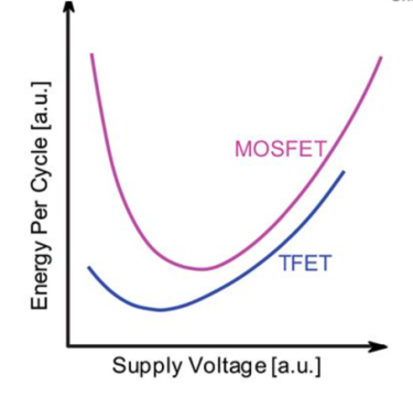
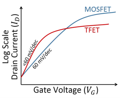
MOSFET has been invented for a few decades and its technology is pretty mature, but today’s engineers meet problems to improve the MOSFET. The first one is the supply voltage. To make MOSFET work properly, the supply voltage has to be greater than the threshold voltage. The supply voltage of MOSFET is not allowed to be reduced infinitely. Decades ago, transistors were still under Dennardian scaling. Thus, the MOSFET can be made smaller with reduced supply voltage. After 2005, in post-Dennardian scaling, the size of the MOSFET was still shrinking, but the supply voltage remains the same [4]. If the power consumption is limited, even though smaller MOSFETs are used in integrated circuits, the certain amount of MOSFETs that are on is fixed, which brings a famous phenomenon called dark silicon: increased transistor density while plenty of transistors stay idle or are not powered for a long time. To solve this problem, some engineers proposed solutions. One of them is called “deus ex machina” [5]. This can be simply understood as changing devices. Due to the innate nature of MOSFET, the supply voltage cannot be reduced to very low amounts as shown in Figure 3. Then, the device can be changed to TFETs, or tunnel FETs. TFETs are based on tunneling effects while MOSFETs are based on thermal injection [6]. TFETs have subthreshold slopes on the order of 30 mV/decade, which is twice as good as the ideal MOSFET, and TFETs have lower on-currents than MOSFETs as shown in Figure 4.
|
|
Figure 3. Energy/cycle - supply voltage of MOSFET and TEFT. | Figure 4. ID - VG of MOSFET and TEFT. |
Summarily, modern MOSFETs face a dilemma due to their scaling down to smaller sizes. On one hand, scaling MOSFETs enables higher device density, improved performance, and lower power consumption. However, as MOSFETs continue to shrink, they encounter several challenges. The shrinking dimensions result in increased leakage currents, causing power dissipation even when the transistor is in the off state. On the other hand, short channel effects arise, leading to degraded transistor performance, such as reduced drive current and increased variability, and the relentless scaling makes it challenging to maintain precise control over the gate oxide thickness, which affects device reliability. Currently, the manufacturing process also becomes more complex and expensive due to the need for advanced lithography techniques and new materials. Overall, while scaling MOSFETs offers benefits, the associated challenges pose a dilemma in terms of power efficiency, performance, reliability, and manufacturing complexity. Researchers and engineers are exploring alternative device architectures and materials to address these issues and sustain the progress of semiconductor technology.
5. Applications
Many semiconductor memory devices, as shown in Figure 5, consist of several basic MOSFET memory cells, such as nonvolatile memory devices. When the gate electrode of a conventional MOSFET is modified so that semi-permanent charge storage inside the gate stack is possible, the new structure becomes a nonvolatile memory device. As the names imply, a volatile memory loses the content, but a nonvolatile memory does not need voltage to maintain the data. There are many different types of nonvolatile semiconductor memory. For example, mask-programmed ROM is fixed by the manufacturer and is not programmable once it is fabricated. EEPROM not only can be erased electrically but also selectively by byte address. Nonvolatile RAM can be viewed as a nonvolatile SRAM, or EEPROM with short programming time as well as high endurance [7].
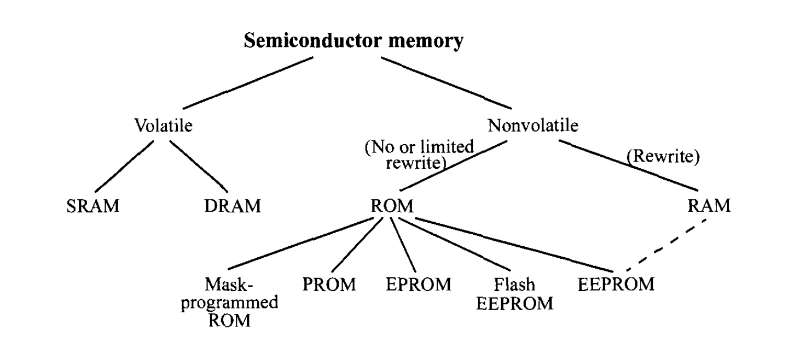
Figure 5. Memory devices.
In today’s world, MOSFETs are used in electric vehicle powertrain systems to control the flow of high-voltage currents. They are employed in motor drive inverters, battery management systems, and charging infrastructure. MOSFETs help optimize energy efficiency, enhance power conversion, and ensure reliable performance in EVs. Designing an EV powertrain primarily focuses on achieving efficiency, as greater efficiency facilitates improved thermal management and enhances the vehicle's range. Insufficient efficiency leads to increased power loss, resulting in additional heat generation, necessitating the enlargement of the EV to accommodate effective heat dissipation. Power density, the amount of power delivered per unit volume of the vehicle, is another crucial factor to consider when optimizing EV powertrains. In order to accomplish these two goals, in addition to powertrain design, semiconductor-based power electronics switches play a vital role in enhancing efficiency and power density. The rapidly increasing demand for electric vehicles (EVs) is driving extensive research into power electronics switches, such as silicon (Si)-based IGBTs and MOSFETs, to enhance switching characteristics and improve overall efficiency [8].
Moreover, there has been a growing interest in the utilization of silicon carbide (SiC) MOSFETs, as shown in Figure 6, due to their potential in enhancing efficiency and reducing the size of power converters: (1) SiC MOSFETs, being wide-bandgap devices, offer numerous advantages that are beneficial to the electric vehicle (EV) industry. They exhibit lower switching and conduction losses compared to silicon (Si) IGBTs or MOSFETs, which are crucial for increasing the driving range of EVs. (2) SiC-based switching devices have a higher junction temperature of 175°C, as opposed to 150°C for Si-based devices. This higher temperature threshold enables the design of integrated powertrains with reduced cooling requirements. (3) Additionally, the high switching frequency of SiC-based devices minimizes the size of passive components like the DC-link capacitor, boost inductor, and EMI filter. These characteristics of SiC-based semiconductor devices contribute to reducing the overall dimensions of the powertrain, thereby indirectly achieving higher power density for an EV [9].

Figure 6. SiC MOSFET structure.
These days, MOSFETs also play a crucial role in LED lighting systems, especially in dimming and color control circuits as shown in Figure 7. They enable precise control of current flowing through the LEDs, ensuring accurate brightness levels and color rendering. MOSFET-based drivers are commonly used in LED bulbs, strips, and displays for residential, commercial, and automotive lighting applications [10]. A MOSFET necessitates minimal current for control (gate voltage) while being capable of supplying significant current to the LEDs. Hence, it is a prevalent setup to utilize the processor for controlling the MOSFET that powers the LEDs. The presence of a resistor serves as a safety measure, ensuring that in the event of MOSFET failure, the processor remains unharmed. For example, the LED driver utilizing SiC MOSFETs in a single-stage configuration occupies 40% less space and weighs 60% less compared to current technology. It also achieves higher efficiency when compared to the two-stage topology using 650V silicon components and the single-stage topology using 900-V silicon MOSFETs [11].
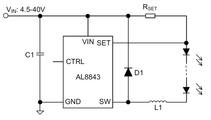
Figure 7. Implementation of AL8843 in LED dimming.
On the whole, MOSFETs are crucial components that contribute significantly to the progress of electric vehicles (EVs). They enable efficient power management and control for motor drives, battery systems, and charging infrastructure, thereby playing a vital role in the advancement of EV technology. Moreover, in memory devices, MOSFETs facilitate high-density storage, faster access times, and low power consumption, which contributes to the development of data storage technology. Similarly, in LED lighting, MOSFETs ensure precise current control, leading to energy-efficient and versatile lighting solutions. These various applications highlight the essentiality of MOSFETs in driving innovation and enhancing performance in the fields of EVs, memory devices, LED lighting systems, and many other areas.
6. Conclusion
In summary, this paper delved into the historical background of transistors and explored the evolutionary path that led to the development of MOSFETs. By highlighting the advantages MOSFETs offer over other transistor types, it became evident that they have become the dominant technology in various electronic applications. However, the current generation of MOSFETs faces challenges that hinder further improvements in their performance. Consequently, addressing these issues becomes paramount for the development of the next generation of MOSFETs. The future research and innovation in MOSFET technology will focus on tackling these dilemmas to enhance performance and pave the way for continued advancements in the field.
However, improving the methodology and finding reliable references are crucial steps for the research of MOSFETs. To enhance research methods and dig deeply into the study of MOSFET, utilizing advanced simulation tools and software can considered to model and analyze the behavior of MOSFETs. These tools provide a comprehensive understanding of the device's performance and allow for the exploration of various design parameters. Consulting books and latest publications from renowned authors and experts can also provide valuable insights into MOSFET technology.
Looking ahead, the study of modern MOSFETs is expected to focus on overcoming the existing performance limitations. This includes addressing issues such as power dissipation, miniaturization challenges, and enhancing overall device efficiency. Emerging research directions may involve exploring novel materials, alternative device architectures, and innovative fabrication techniques to further advance MOSFET technology. Additionally, the integration of MOSFETs with other emerging technologies like nanoelectronics, photonics, and quantum computing is likely to shape the future of MOSFET research.
Acknowledgements
I would like to express gratitude to my supervisor, Prof. Yiyu Shi, and teaching assistant, Devin, for providing me with background knowledge in integrated circuit design.