

1. Introduction
The IIC bus is a bidirectional serial bus protocol for chip-to-chip connections, which was developed by PHILIPS (now NXP) company as a peripheral bus [1]. It has gained widespread use due to its unique and simple structure, and almost all SoCs use it. The protocol has been widely applied in various industries such as video, audio, IC card, banking card, household appliances, communication equipment, and various electronic products and devices. It has also been widely used in the fields of intelligent instruments and measuring instruments.
The Inter-Integrated Circuits (IIC) is a popular two-wire bus used in the IC industry, allowing bidirectional communication. Each device connected to the IIC bus has a specific address, and the IIC supports multi-master operations with arbitration features. Slaves on the IIC bus can act as transmitters or receivers. Operating at low to medium speed, IIC boasts several distinct features, including resistance to noise and glitches, robustness, and the ability to use bus extenders for long-distance communication. These extenders also allow for flexible communication, catering to users’ specific requirements [2].
Under this protocol, only two signal lines, i.e., one clock line SCL and one data line SDA, are needed to achieve duplex synchronous data transmission and to interconnect 128 different devices together extremely conveniently to form a multi-computer system and a peripheral device expansion system. The hardware system has a simple and flexible expansion method[3].The external hardware requires only two pull-up resistors, one on each line. All devices connected to the bus have their own address, and the IIC module has a master-slave transfer mode. There are four possible modes of operation for a device in the system: host transmit, slave transmit, host receive, and slave receive[4] . Siemens (previously Mentor Graphics) developed ModelSim as a multi-language simulation environment for hardware description languages like VHDL, Verilog, and SystemC. ModelSim also features a built-in C debugger. It can be used as a standalone tool or integrated with software like Intel Quartus Prime, PSIM, Xilinx ISE, or Xilinx Vivado. With its robust verification capabilities, ModelSim is an excellent choice for verifying FPGA designs of small to medium size.
2. Principle of iic bus protocol
2.1. Basic characteristics
Only two buses are required: a serial data line SDA (hence half-duplex), and a serial clock line SCL. Each device that is connected to the bus can be addressed with a unique software address and operates in a simple master/slave relationship, with the master device capable of acting as a master transmitter or master receiver. This is a multi-master bus, which means that if two or more masters attempt to initialize communication simultaneously, collision detection and arbitration can prevent data transmission from being corrupted. The standard mode for bidirectional data transfer is 8-bit serial with a maximum bit rate of 100kbit/s. For faster data transfer, the fast mode offers up to 400kbit/s, while the high-speed mode can achieve up to 3.4Mbit/s.The maximum number of ICs that can be connected to the bus is determined by its 400pF capacitance limit [5]. The IIC interface consists of a clock line (SCL) and a data line (SDA). Both lines are open-drain or open-collector structures and require external pull-up resistors to mount multiple devices. Each device has its own address, and the host selects different devices through different addresses [6]. As shown in Figure 1.
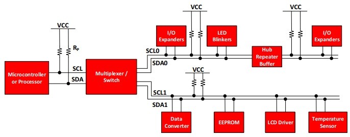
Figure 1. IIC structural interface diagram.
2.1.1. Advantages of the IIC bus. The main advantage of the IIC bus is its simplicity (IIC has only two signal lines) and effectiveness (determined by the clock line on the SCL line). MCUs with IIC bus interface can directly connect to various expansion devices with IIC bus interface (such as memory, I/O chip, A/D, D/A, keyboard, display, clock, etc.). Since the IIC bus uses a pure software addressing method, there is no need to connect chip select lines, which greatly simplifies the number of buses. Another advantage of the IIC bus is that it allows multiple master devices. Any device that can send and receive can become a master bus. A master controller can control the signal transmission and clock frequency, and there can only be one master controller at any time point. In practical applications, it is often encountered that the microcontroller is the master device and other peripheral interfaces are slave devices.
2.1.2. Disadvantages of the IIC bus. In standard IIC normal mode, the data transfer rate is 100kbit/s, and in high-speed mode it can reach 400kbit/s. The number of peripheral devices connected by IIC is not unlimited, and the number of extension cycles on the bus is limited. The number of extended cycles on the bus is not determined by current load, but by capacitive load. Each device interface on the IIC bus has a certain equivalent capacitance. The more devices (extended peripheral devices can be seen as parallel to the main device’s bus), the larger the capacitance value will cause signal transmission delay. The number of devices allowed to connect to the bus does not exceed 400pF (the capacitance of the bus can be increased by other methods), based on which the length of the bus and the number of extended peripheral devices can be calculated [7].
2.1.3. Comparison with other serial port protocols. UART: Universal Asynchronous Receiver/Transmitter SPI: Serial Peripheral Interface. USART: Universal Synchronous Asynchronous Receiver/Transmitter.
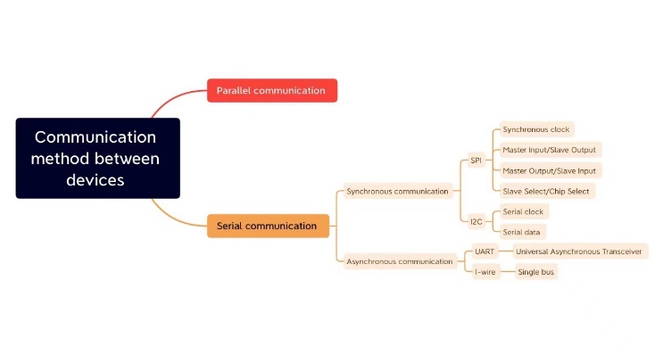
Figure 2. Classification of common communication modes.
UART is a universal asynchronous serial port, not fast, can be full duplex, structure generally consists of baud rate generator, UART transmitter, UART receiver, hardware two wires, one receive and one send. SPI is a high-speed synchronous serial port, high-speed, full duplex, independent transmission and reception, synchronous interface, can realize interconnection of multiple SPI devices, hardware 4 wires. As shown in Figure 2. IIC is a bidirectional, two-wire, serial, multi-master interface standard. Not fast speed,half duplex,synchronous interface with bus arbitration mechanism. It is very suitable for frequent data communication between devices at close range and can realize device networking [8]. IIC combines the advantages of SPI and UART. With I2C protocol, it is possible to connect several slave devices to a single master device, and multiple master devices can control one or more slave devices.
2.2. IIC sequence base unit
Relationship of controlling: At any time, it is the master that completely controls the SCL line. In idle moments, the master can actively initiate control of SDA. Only when the slave sends data and the slave responds, will the master transfer control of SDA to the slave. The slave is not allowed to initiate control of SDA actively. Start condition and stop condition: Beginning condition: While SCL is at a high level, SDA transitions from a high level to a low level.Ending condition: While SCL is at a high level, SDA transitions from a low level to a high level.
.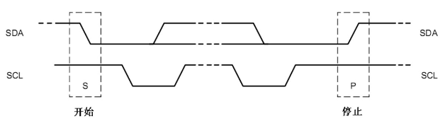
Figure 3. Beginning condition and ending condition.
Data transmission: Data and address are transmitted in 8 bits/bytes, with high bits first. The one byte following the start condition is the slave address. After 8 clocks of a byte transmission, during the 9th clock period, the receiver must send back an acknowledge bit (ACK) to the sender [9]. As shown in Figure 3.
To send a byte, the master sends data bits on the SDA line during the SCL low level, starting with the high bits. The master then releases the SCL, allowing the slave to read the data bits during the SCL high level. It’s important to note that the SDA line shouldn’t have any data changes during the SCL high level. This process is repeated 8 times to send a byte. When a byte is received, the slave will transmit data bits on the SDA line one by one, starting with the most significant bit, while SCL is at a low level. After transmitting all 8 bits, the slave releases the SCL line. During the subsequent high level of SCL, the master reads the data bits from SDA one by one, and SDA must not be changed during this period. This process is repeated 8 times to receive a complete byte. (It is important for the master to release the SDA line before attempting to receive the byte). The acknowledge bit is used in communication between the master and the slave. When the slave sends a byte of data to the master, it sends an additional bit of data in the next clock cycle. A value of 0 in this bit indicates that the data has been received and acknowledged, while a value of 1 indicates that the data was not acknowledged. On the other hand, when the master sends data to the slave, it waits for an acknowledgement bit from the slave in the next clock cycle after sending a byte [10]. As shown in Figure 4. A value of 0 in the acknowledgement bit indicates that the data has been successfully received, while a value of 1 indicates that the data was not acknowledged (the master must release the SDA line before receiving the acknowledgement bit).
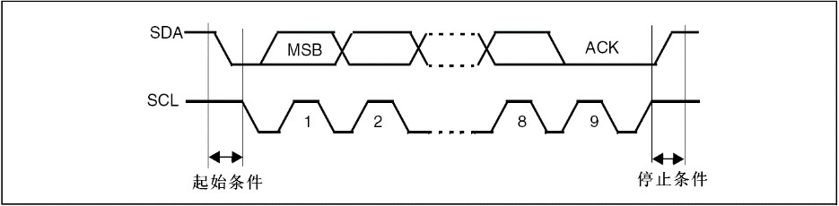
Figure 4. Data transmission.
3. Code implementation and the simulation
3.1. Code implementation
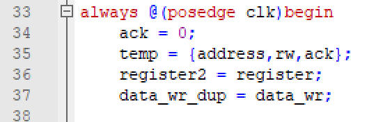
Figure 5. Assembly data.
The section in figure 5 defines three data: temp consists of slave address, read/write bit and acknowledge bit, register2 is the address of register in slave, data_wr_dup is the data to be transmitted.
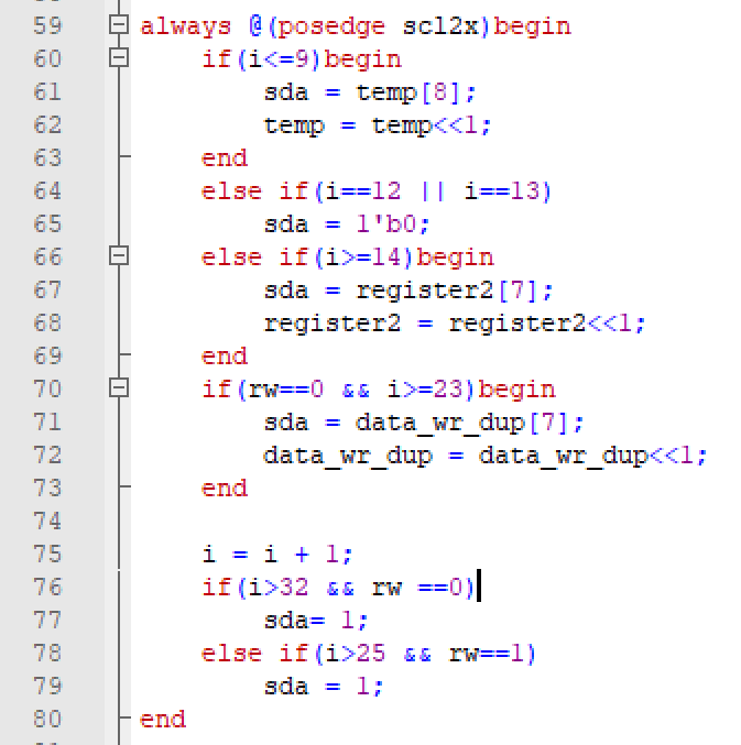
Figure 6. Data transmission.
The part of Figure 6 implements the data transmission, all data are sent with high bit first, i is used for counting, first send slave address, read/write bit and acknowledge bit [11]. Then wait until the count reaches 14 to continue sending slave register address, this process simulates the acknowledgment of slave after receiving the address sent by master. Finally, send the data to be transmitted immediately.
This part is used to determine the data to be transferred, selecting the slave and slave registers. IIC complete sequential waveform, As shown in Figure 7.
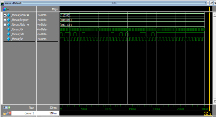
Figure 7. The simulation in modelsim.
This waveform shows the master writing data to the slave at address 105, the target register at address 0100101 and the data to be written at 25. After the initial condition, the slave address is sent first and the slave’s reply process is simulated by waiting for several cycles of signals, after which the slave register address and the data to be written are sent. Through repeated implementation of the above process, the communication between the master and the slave can be realized.
4. Conclusion
When using IIC protocol for communication, some errors may occur, such as data loss, communication timeout, etc. In order to ensure the correctness of data transmission, these errors need to be handled, such as resending data, waiting for data arrival, etc. In this paper, delved into the principles and implementation of the IIC protocol. By introducing the working flow, transmission modes, and application scenarios of the IIC bus, the widespread application of the IIC protocol in modern digital systems can be seen. From microcontrollers to sensors, from embedded systems to industrial automation, the IIC protocol has become an important digital communication interface. During the research process also noticed some challenges and limitations in implementing IIC, such as the tight timing requirements, the speed limit of data transfer, and the reliability issue in long-distance communication. Therefore, when designing and using the IIC interface, these issues need to be carefully considered, and appropriate testing and verification should be carried out in practice. As digital systems and the Internet of Things continue to evolve, the IIC protocol will continue to play an important role. There are more research and improvements in the future, making the IIC protocol more efficient and reliable in meeting the needs of digital systems and the Internet of Things. Generally speaking, learning IIC protocol requires mastering the knowledge of hardware connection, communication mode, register setting and error handling. It is necessary to understand and adjust the specific hardware devices and application scenarios to ensure the correctness and reliability of data transmission.