


1. Introduction
Electric vehicles (EVs) offer numerous advantages over traditional vehicles, including reduced emissions, enhanced energy efficiency, and lower operating costs. The global adoption of EVs is accelerating, with sales projected to reach approximately 17 million by the end of 2024, representing over 20% of global car sales, understanding their growing popularity. [1]. Printed-circuit-board (PCB) is the core of the EV operating system, which serves as the foundation of electronic systems [2]. PCB plays a crucial role in integrating and managing a large number of electronic components that are essential for functions ranging from power distribution to vehicle control systems.
Electromagnetic interference (EMI) affecting PCBs in EVs primarily originates from two sources: the vehicles' motor drive system and internal PCB circuitry. Strong EMI can lead to signal distortion and cause the malfunction of the PCB. In such cases, electronic equipment can negatively influence each other, affecting the normal operation of electronic equipment and instruments. In serious situations, this can threaten the operational safety of EVs.
Mitigating EMI enables the automobile PCB to better transmit signals and data, reduce signal loss and interference, improve electromagnetic compatibility (EMC), and degrade radiation levels [3]. The mitigation of EMI is essential for improving the maneuverability, acceleration, and overall performance of the vehicle. Through the design and production of high-quality PCB, the normal operation and coordination of these safety systems can be ensured, thus providing vehicle stability, brake safety, and occupant protection. Currently, research on the analysis and optimization of electromagnetic interference in electric vehicles focuses mostly on the interference source and propagation path, with a lack of research on protective solutions for individual sensitive devices such as PCB on EVs.
This paper reviews the current state of research and assesses the feasibility and effectiveness of various EMI mitigation strategies. Section II presents the principle of EMI generation and dissemination, the source of EMI in EVs and the impact of EMI on PCBs. In Section III, effective solutions from the three perspectives are presented—suppressing the generation of EMI from noise sources, reducing EMI on EMI propagation paths, and optimizing PCB design. In addition, advantages and disadvantages of the above methods are discussed, along with possible application scenarios. By integrating these insights, this article aims to provide feasible suggestions for ensuring the efficient and stable work of PCB in EVs and improving the reliability, efficiency and safety of EVs.
2. Electromagnetic interference in electric vehicles
Electromagnetic interference (EMI) refers to the interference effect of electromagnetic waves generated by electromagnetic induction effect on other electric devices in the environment during the normal operation of electric devices or systems. The two types of EMI are radiation emission (RE) and conducted emission (CE), depending on the electromagnetic interference's transmission channel. The transmission path of CE includes wires or common ground wires, which can be transmitted through space radiation or near-field coupling. RE is generally transmitted in space in the form of electromagnetic coupling, and shielding materials are used to prevent or reduce energy transmission in space.
The drive system of electric vehicles (EVs) is the main source of EMI of EVs, consisting of high-power electric devices, including power batteries, high-power DC/DC converters or DC/AC inverters, drive motors and their connected high-voltage cables. When these power electric system work, it will emit strong electromagnetic interference, forming a complex electromagnetic environment. During the breaking process of the switching element, due to the jump in voltage and current in a short period of time, the \( \frac{du}{dt} \) of many switching elements reaches tens of thousands of volts per microsecond, and the operating frequency of the switch also reaches tens of kilohertz, thus forming strong radiation and conductive electromagnetic interference. On the other hand, high-voltage cables are used to link the power drive components. When operating, a significant amount of current—hundreds of amps—flows, and the variations in that current generate a strong electromagnetic radiation. When these EMI noises spread, they can influence various electric devices and receivers installed in EV systems, resulting in malfunctions or performance degradation. The block diagram of the plug-in hybrid electric vehicle (PHEV) configuration is depicted in figure.1 [4].
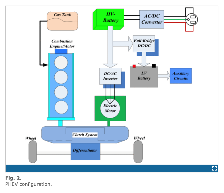
Figure 1: PHEV configuration [4]
In addition, the PCB will be interfered with and emit electromagnetic radiation internally. According to the basic theory of electromagnetic field, when there is RF (radio frequency) current in the external transmission line or PCB printed line, the current from the current source to the load must be returned to the current source through the return path, so that the formation of a closed current loop will generate a magnetic field, which will also generate a radiation electric field, and then form EMI[5.6.7].The key to the electromagnetic compatibility design of PCB is how to reduce radiation ability and how to improve anti-interference ability. Reasonable layout and wiring are the guarantee of the design of the PCB.
3. Mitigative solutions
3.1. Suppressing main electromagnetic interference sources
Unlike traditional engine vehicles, electric vehicles integrate a number of high-voltage components. This section will focus on how to prevent these components from generating EMI interference sources. For switched-mode power supply, technologies such as parallel capacitive coupling, frequency hopping, and digital active EMI filtering have been identified as effective solutions to reduce high-frequency noise and improve system stability. In the context of CAN bus interference, the use of electrical isolation means and shielded twisted pair is essential to maintain data transmission integrity and reduce overall system outages. In addition, suppressing the EMI of the low-voltage battery pack is also an important part. By implementing these strategies, engineers can achieve a higher level of interference control, resulting in stronger and more stable electronic systems within electric vehicles.
3.1.1. Suppression of electromagnetic interference from Switched-Mode Power Supply (SMPS)
3.1.1.1. Parallel capacitive coupling (Cx)
The switching operation of DC/DC converters generates significant EMI, especially during the start and brake phases. These conditions place high load requirements on switching power supplies, resulting in increased interference levels on positive high-voltage power lines [8].
If we want to tackle this EMI issue head-on, we need to focus on dealing with specific frequency resonators, like the troublesome 2 MHz one. By eliminating or reducing the resonant amplitude of 2 MHz, the conduction voltage can be controlled within an acceptable range. Reducing equivalent parasitic inductance Ls of the DC filter capacitor CDC is to make the resonant point shift from 2 MHz to a high frequency band of about 10 MHz. Here we can choose a parallel 1uF X capacitor CX and CDC, and its parasitic inductance LCX is 10nF, as shown in Fig 2 [9].
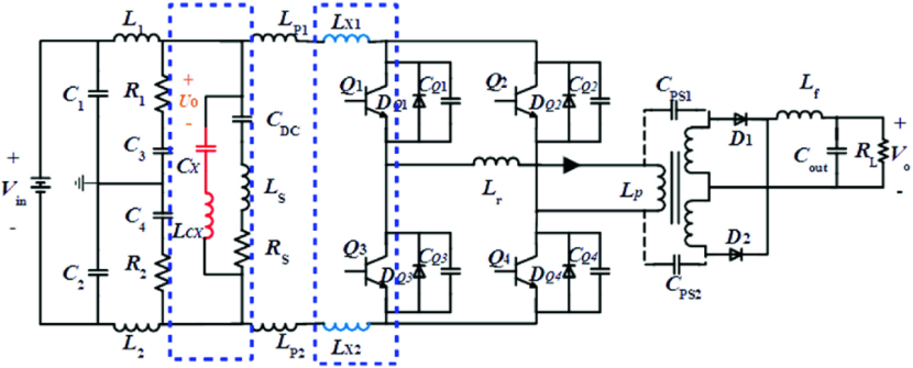
Figure 2: Filter circuit to reduce the peak of the resonance point at 2MHz
The advantage of using this method to design the filter circuit on the PCB of the DC-DC converter is: mitigating the electromagnetic coupling between the filter input and output cables; The design size is significantly reduced to only about one-fifth of the high-voltage filter (as shown in Fig 3), greatly simplifying engineering design.
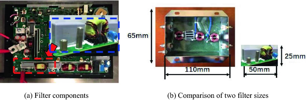
Figure 3: Filter circuit on the PCB
3.1.1.2. Add the frequency hopping technique
Through manipulation of the switching signal frequency, it becomes possible to minimize the peak of the power spectrum. The integration of a frequency hopping control module into the traditional DC-DC converter schematic enables precise control over the generation of sawtooth waves at varying frequencies. The frequency of these sawtooth waves dictates the central switching frequency of the DC-DC converter. Scanning through 8 different switching frequencies theoretically reduces the power spectrum at the DC-DC converter output node by up to 18 dB [10].
3.1.1.3. Digital Active Electromagnetic Interference Filtering (DAEF) technique
The Digital Active EMI Filtering (DAEF) technique represents a groundbreaking advancement in SMPS conducted EMI suppression technology. This paper [11] introduces a novel DAEF topology that possesses the capability to effectively suppress both common mode (CM) and differential mode (DM) EMI while preventing any conversion between them. The DAEF topology planning is shown in Figure 4. It includes electromagnetic interference signal detection circuit, ADC sampling circuit, DAC output and decoupling circuit between injection point and sensing point, the DAEF system stands as a versatile solution for EMI mitigation and management.
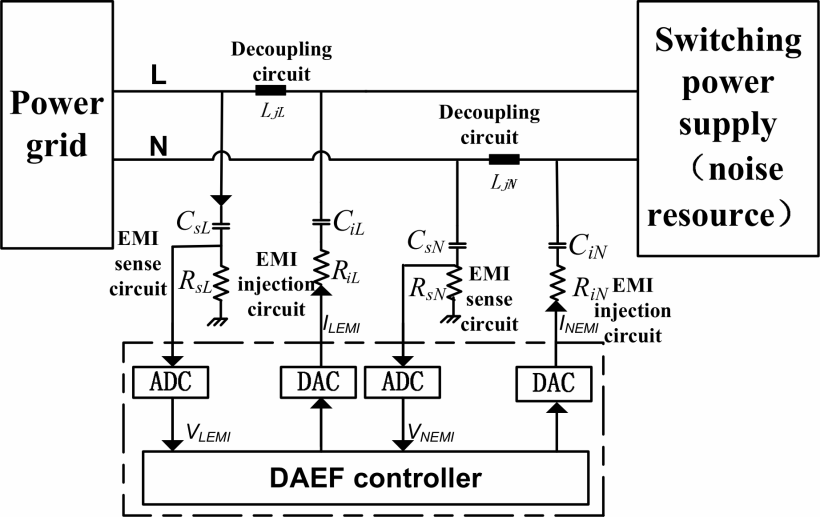
Figure 4: General scheme of proposed DAEF
The electromagnetic interference detection circuit is an RC high-pass filter composed of resistance and capacitance. By designing decoupling circuit, the coupling between signal sensing point and signal injection point can be effectively reduced. The electromagnetic interference injection circuit can be partially designed by an RC low-pass filter. Integrating the DAEF controller into the inherent controller of the power converter proved to be a cost-effective solution, ultimately reducing the overall expenses associated with the power converter. In addition, placing a high-impedance RF inductor as a decoupling circuit between the injection point and the induction point can effectively reduce the coupling between the two points and further improve the filtering performance.
3.1.2. Suppression of electromagnetic interference from CAN bus
In addressing the suppression of EMI from the CAN bus, it is essential to fortify each node's anti-interference capabilities. Opting for a CAN repeater, a CAN interface card with photoelectric isolation, and a CAN/485 conversion module allows for electrical isolation of network terminal equipment. This isolation prevents any discrepancies in reference ground potential from impacting other devices, ensuring that interference does not infiltrate the control circuit and thereby safeguarding the control system's integrity [12].
3.1.3. Suppression of electromagnetic interference from low voltage battery pack
This study presents an embedded DAEF that can be seamlessly integrated into digital controllers of DSP-based DC converters designed for low-voltage battery pack charging in electric vehicles. Figure 5 depicts the layout of the Converter closed loop block diagram, which consists of two digital control loops embedded in the DSP device, each of which acts on the power converter.[13]
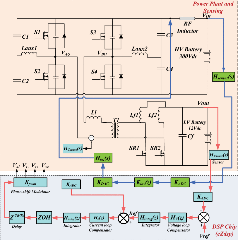
Figure 5: Converter closed loop block diagram
3.2. Reducing electromagnetic interference noise on propagation paths
The above section has introduced three methods for suppressing main EMI source,cutting off the EMI propagation path is also important way to mitigate EMI.Shielding techniques are main method of cutting off the EMI propagation path,Figure.6[14] shows the mechanism of EMI shielding,EV’s internal High-current components and weak current components need different shielding methods,high-precision equipment inside EVs such as driving computers, the control signal of this equipment is relatively weak, Usually it uses metal shell shielding technology, some additional charging devices, traditional wired charging pile and wireless charging pile,These high-power equipment will interfere with the electronic equipment in EVs, now it can be shielded with aluminum plate, this section reviews the traditional feasible methods used on EVs such as metal shell shielding and high-current and weak current separation shielding techniques, but also puts forward some small number of popular or gradually put into use methods, these methods have good prospects for development, such as high-permeability magnetic materials, Ferrite applications in EVs.The following table.2 shows the methods of reducing EMI noise on propagation paths.
Table 1: approaches of reducing EMI noise on propagation paths
Methods | ||
Shielding Techniques | Metal Shell Shielding | [15,16] |
Ferrite Shielding for Wireless Power Transmission | [17] | |
Multilayer Shielding | [18-20] | |
Suppression of EMI from Motor Drive System | Using X and Y Capacitors | [21] |
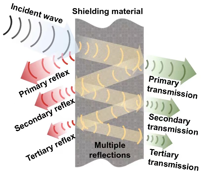
Figure 6: EMI shielding mechanism based on transmission line theory [14]
3.2.1. Shielding techniques
3.2.1.1. Metal shell shielding
Metal shell shielding techniques are traditional and in EVs they are widely used, conductive cavity can be applied to protect the sensitive equipment in EVs. The purpose of metal shell shielding is to prevent the external electric field from entering a specific area and place the cavity conductor. Under the action of the external electric field, the surface charge of the metal parts will be redistributed until the internal field strength is zero everywhere. The use of grounded closed metal shell as a cavity conductor to shield the external electric field is a good electrostatic shielding method in EVs, usually metal shell with low resistivity metal materials such as aluminum [15] or iron aluminum alloy, in EVs, metal shield shell [16] is often used in motor, inverter shell and other key components, but if the metal shell is not fully closed, the shell has holes. Although it can also play a role in electrostatic shielding, it destroys the conductive continuity of the shield, and non-conductive gaps or holes may lead to electromagnetic leakage and electromagnetic pollution.
3.2.1.2. Ferrite shielding for wireless power transmission
Static magnetic field is the magnetic field generated by constant current or permanent magnet, low frequency magnetic field shielding refers to the low impedance shielding cavity and protection space used in parallel, low frequency magnetic field always tends to preferentially pass through the low impedance shielding cavity, thus protecting the device in the protection space, the use of iron, nickel and other high permeability magnetic alloy made of shielding cover, is the traditional magnetic field shielding practice, but compared with electrostatic shielding, The difference between the conductivity of ferromagnetic material and air is much smaller, magnetic shielding will always produce some magnetic leakage, although the use of multi-layer shielding to achieve a better shielding effect, but the magnetic shield becomes more bulky, affecting the driving effect of electric vehicles. Most EVs use aluminum plates between the transmitter and receiver of the wireless charging system to shield the magnetic field. In a study on the application of ferrite [17] as a magnetic field shield material in the wireless power transmission system, the advantages of ferrite compared with traditional magnetic field shield materials were demonstrated, and the magnetic field shielding effect of the wireless power transmission system was improved.
3.2.1.3. Multilayer shielding
MXene, a new family of 2D materials, has been found to have excellent electromagnetic shielding properties due to its excellent electrical conductivity, MXenes has a higher dielectric mass than graphene [18], so they have stronger conductivity, and the porous structure of MXenes [19] has better EM absorption capacity than the layer structure. This article analyzes the present study of MXene and graphene applied to porous composites, a benefit of using multilayer shielding is that reflections can be minimized, and as the number of layers increases, the shielding efficiency of EMI can be increased to more than 80dB [20].
3.2.2. Suppression of electromagnetic interference from motor drive system
The conducted emissions from the motor driving system can disrupt other systems in electric vehicle. Addressing this issue, the paper [21] proposes a series of low-cost EMI mitigation techniques.
To mitigate EMI from the high-voltage (HV) parts in the motor driver system, the use of X and Y capacitors is recommended.
X capacitors and Y capacitors are important safety capacitors in power electronic equipment, which are used to eliminate common mode interference and EMI in power grids, respectively. X capacitor is mainly used to filter and reduce the influence of high-frequency noise on the circuit to ensure the stable operation of the equipment; The Y capacitor mainly inhibits the common mode interference, improves the anti-interference ability of the equipment, and ensures the safety of use in the ground circuit. In Figure.7[21], two Y capacitors are deployed for each HV port to filter common-mode noise, while an X capacitor is employed to address differential-mode noise. These capacitors function effectively as first-order filters and are implemented at a low cost without the need for inductors.
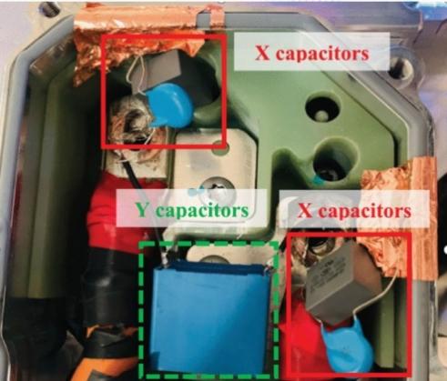
Figure 7: EMI path of the common mode and differential mode [21]
The implementation of this measures can enable EMI measurements to meet the requirements of CISPR 25 Level Ⅲ and even level Ⅴ in some frequency bands.
The first two parts have introduced feasible EMI mitigation methods from suppressing main EMI source and cutting off EMI propagation paths, the next part will cover some methods to mitigate EMI from PCB design perspective.
3.3. PCB electromagnetic compatibility design
Compared to other electric devices such as electric motor system and batteries, the PCB produces relatively low levels of EMI. However, due to the small scale of PCB, even this small amount of EMI can have a significant impact on PCB itself. To address this problem, this section summarizes the methods to mitigate EMI noise in EVs. Generally, the mitigation techniques can be classified into two primary categories. The following table outlines the approaches along with their references.
Table 2: Approaches of PCB EMC design
Methods | ||
Layout and Routing | High-Frequency Signal Line Arrangement | [12,23,24] |
Component Layout | [23,25-27] | |
Power Plane Design | [12,26,28-31] | |
Stack-up Design | [28,34] | |
Via (Via-hole) Design | [32] | |
Grounding | Reduce Ground Line Impedance | [26,35,36] |
Ground Plane Position and Design | [35,37] |
3.3.1. Layout and routing
Improper layout or routing is the major cause of electromagnetic interference, particularly in digital analog hybrid layouts [22]. Therefore, proper layout and routing are crucial for reducing EMI.
When integrating low-speed, medium-speed, and high-speed circuits, it is crucial to separate low-level analog circuits from digital circuits as much as possible. This layout shortens the path of high-frequency currents on the printed circuit board (PCB), which helps mitigate the noises within the board [23].
EMI issues in PCB mainly include common impedance coupling, radiation from high-frequency signal lines, crosstalk and the induction of high-frequency radiation by printed traces [22]. Among these, radiation from high-frequency current-carrying lines has the most severe impact, so special consideration should be given to the placement of high-speed signal transmission lines during layout and routing. Here are some common principles for routing:
3.3.1.1. High-frequency signal line arrangement
PCB routing should avoid the crosstalk caused by close parallel routing of signal lines, especially the clock lines, as they usually have the highest frequency [23]. If parallel routing cannot be avoided, the distance between parallel signal lines should be increased. If the space between signal lines reaches 3W (W is the width of the signal line) 70% of crosstalk issues can be eliminated, while spacing them at 10W can eliminate 98% [24]. If two signal lines are close together, a ground line should be routed between them, or large area copper ground should be laid on adjacent layers to reduce inter-line crosstalk. Additionally, high-frequency signal lines should use smooth arcs and avoid using 90-degree bends to minimize reflections caused by abrupt changes in the he transmission line's characteristic impedance [23].
Because the clock lines usually have the biggest EMI impact, special method is needed. By adding magnetic beads, clock interference signals on the PCB can be suppressed. These beads are heated to dissipate the high-frequency current. Filtering ability of the bead is related to the frequency, material, bead size and the current. The principle behind choosing beads for EMI suppression is that they have the highest impedance at EMI noise frequencies. Different types of magnetic beads can be selected according to specific design requirements [12].
3.3.1.2. Component layout
Closely related components should be placed together to keep high-speed lines as short as possible. For high-current components such as relays, indicator lights, and speakers, their ground lines should be routed separately to reduce noise on the ground lines [23]. Increasing the distance between components that generate strong radiation electromagnetic fields and those sensitive to electromagnetic induction is an important way to reduce interference between components on the PCB. Additionally, the crossing of high and low voltage components and strong and weak signal components should be avoided [23,25]. If small signal amplifiers are equipped on the board, the weak signal lines before amplification should be kept away from strong signal lines and, if possible, shielded by ground lines [26]. Furthermore, components that generate magnetic fields, such as transformers, speakers, and inductors, should be oriented to reduce the amount of the printed conductors that cut into the magnetic field lines. The magnetic field directions of adjacent components should be perpendicular in order to minimize mutual coupling.
To minimize the effects of overheating, high-power transistors, high-power ICs, and high heat-generating components should be positioned in easily heat-dissipating areas [26]. As for crystal oscillators, they should be placed as close to integrated circuits as possible, and crystal oscillator case should be grounded [23,27].
3.3.1.3. Power plane design
The power layer shall be adjacent to and below the ground layer. Each power supply pin should have a decoupling capacitor of 0.01F to 0.1F, and the decoupling capacitor should be placed as close to the individual pins as possible [28]. The inclusion of decoupling capacitors in the lower power layer can introduce additional charge reservoirs to compensate for potential signal voltage dips, thus mitigating the impact of switching noise [29]. Moreover, minimizing the distance between the noise source and the decoupling capacitor is also an effective meethod for ensuring good signal trasmission [29].
Reference [12] proposes a decoupling capacitor selection method based on geometric average resonance points. When two different capacitors are connected in parallel, two anti-resonant points and one resonant point appear on the impedance curve, as shown in Figure.8. The received self-resonant frequency of the decoupling capacitor can be equal to the average frequency of two adjacent anti-resonant points where the decoupling capacitor is placed. By calculating the geometric mean of these three points, the minimum impedance peak on the impedance curve can be found and the appropriate decoupling capacitance can be selected. With regard to the placement of decoupling capacitor, the distance between the surface-mount power supply pin and the decoupling capacitor should not exceed the decoupling radius of the capacitor.
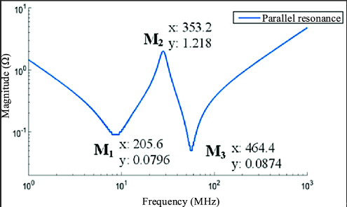
Figure 8: Impedance curve of two different capacitors in parallel [12]
The electric field between the power plane and ground plane is variable, causing electromagnetic interference radiation at the edge of the board, known as the edge effect, as shown in Figure.9. Pull back one of the planes can reduce edge effect. Retracting the power plane by 20H (H is the dielectric thickness between the power and ground planes) can confine 70% of the electric field within the ground edge while retracting by 100H can confine 98% [26,30,31]. (Figure.10)
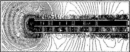
Figure 9: Coupling along PCB edge [31]
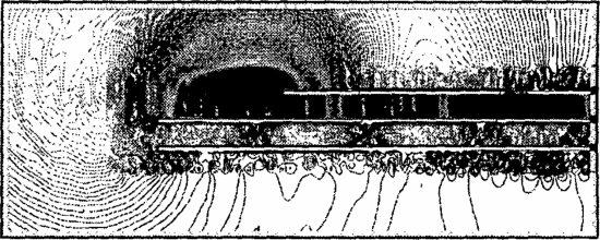
Figure 10: Edge emission with retracing design [31]
3.3.1.4. Stack-up design
Stack-up arrangement is also a factor affecting PCB EMC. To ensure good electrical performance, cross-section of each routing layer must be well-designed [28]. The layer stack should follow symmetry principles. The distance between the power plane and its corresponding ground plane should be minimized to form an effective planar capacitor., reducing power plane impedance [34]. Figure.11 shows a schematic of symmetrical layer stack design.
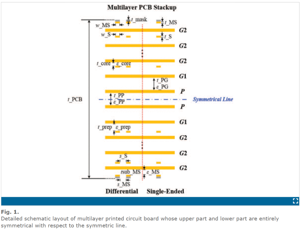
Figure 11: A stack-up solution [38]
All signal layers should be adjacent to their corresponding ground planes, avoiding adjacency of two signal layers [34]. Symmetrical layering design can eliminate open edge effects, which confines resonance energy to the power-ground plane. The copper plating process can connect the edges of two ground planes, thus eliminating open edges [34]. Figure.12 shows the schematic of symmetrical layer stack design and reducing electromagnetic interference by eliminating open edges.
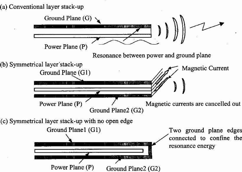
Figure 12: Symmetrical layering design [34]
3.3.1.5. Via (Via-hole) design
Excessive via spacing can cause electromagnetic leakage. However, in real cases, vias cannot always be placed at minimum spacing or placed regularly, so the maximum spacing should be constrained based on the actual circuit board situation. Literature [32] suggests that the distance should be: l< \( \frac{λ}{10} \) ~ \( \frac{λ}{100} \) (generally, l < \( \frac{λ}{30} \) ), where l is the distance (m) and λ is the wavelength (m) [32]. To ensure good contact between the PCB and fixtures, edge via band design should also be considered [32].
3.3.2. Grounding
Grounding is another critical issue in PCB EMC design. Proper ground layer layout helps eliminate magnetic flux in multilayer PCBs, and a complete ground layer effectively reduces noise emissions across all frequency bands [33]. Here are several key principles of grounding:
3.3.2.1. Reduce ground line impedance
PCB ground impedance is a primary cause of radiated EMI, espicially for frequencies above 30 MHz [35]. Ground currents cause antenna effects when flowing through ground lines. Placing circuits with significant interference emissions closest to the confluence point reduces trace length and increases trace width [36], thereby limiting common impedance coupling by limiting noise circuit return path impedance. Additionally, copper plate on PCB ground planes reduces ground line impedance, enhances anti-interference capability [26]. A cross capacitor can be added between the output and input, and an impedance resonance network can be created to lower the ground impedance [36].
3.3.2.2. Ground plane position and design
For multilayer boards, a complete ground plane should be reserved in the PCB, with important signal lines adjacent to this layer, and it is better to put the ground layer loser to the clock source than to the antenna.
For projects with both digital and analog components, their grounds should be set separately (as shown in Figure.13) [35, 37]. Analog and digital grounds need to be connected, commonly through 0-ohm resistors, ferrite beads, inductors, capacitors, or A\D converters [37].
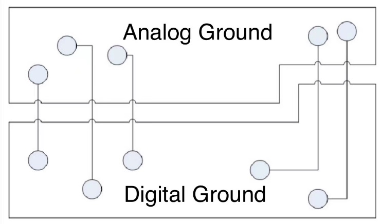
Figure 13: Ground setting [37]
4. Conclusion
This paper first reviews the sources of EMI in EVs, discussing their generation principles and propagation mechanisms. It also summarizes the current research in the field of PCB EMC design within EVs. An extensive evaluation of diverse EMI mitigation strategies was conducted for EV propulsion systems, encompassing tactics from diminishing noise origins to inhibiting propagation routes and optimizing PCB layouts. This analysis aimed to alleviate electromagnetic interference comprehensively. The successful implementation of these mitigation strategies is anticipated to significantly enhance the reliability, efficiency, and safety of EVs.
In recent years, the research on the electromagnetic interference mechanism of motor drive systems has gradually matured, and the research on EMC predictive modeling simulation and EMI suppression technology is still under development. Due to the EMI mechanism of the motor drive system and the complexity of the system, it brings great difficulties to accurate modeling. How to accurately establish an EMI prediction simulation model of the motor drive system and effectively guide the engineering application is still an urgent problem that needs to be solved. In addition, the EMI suppression technology of the motor drive system is mainly used in practice. In the stage of laboratory research and exploration, a relatively complete solution has not been formed. How to comprehensively consider EMC characteristics in the process of product design and application, and develop corresponding design theories and specifications, which should be solved in future engineering applications.