


1. Introduction
Amplifiers have become essential in various fields. For instance, in wireless communication, the variable gain amplifier can automatically adjust the gain based on the strength of the received signal to ensure effective reception at different strengths and distances. A scholar has identified the variable gain amplifier as a crucial module for controlling RF/IF signal power at an optimal level in the RF system [1]. In audio devices, gain amplifiers enhance sound signals by increasing volume or power, reducing noise and distortion, and improving audio clarity to make them more easily perceived by the human auditory system. Moreover, in medical devices, amplifying biological signals (ECG/EEG) enables doctors to obtain more accurate biological signal data and improve diagnostic accuracy [2]. The examples mentioned above are just a few common instances where amplifiers play a significant role. There is an increasing amount of research on amplifier gain. For example, Yang Fan et al. proposed an improved operational transconductance amplifier based on a collapsible cascode structure that can increase the gain bandwidth product of the amplifier by about nine times compared with traditional cascode structures[3].Additionally, Zheng Kailun et al. utilized gain bootstrap-up technology under traditional OTA structure and RFC structure for auxiliary op amp to achieve higher DC gain[4].These scholars have innovated basic circuit structures to further improve circuit gain. Through theoretical derivation and simulation of the cascode structure, five-transistor OTA and cascade structure, this paper explores the effect of these basic circuits on gain improvement.
2. Circuit derivation and simulation
2.1. Common source differential amplifier circuit
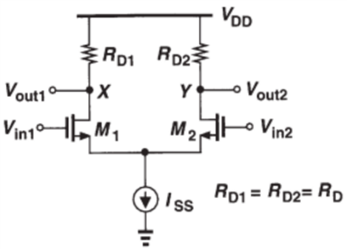
Figure 1. Common source differential amplifier circuit.
In Fig.1, the common-source differential amplifier circuit is composed of two NMOS, M1 and M2. ISS is the tail current source, whose function is to suppress the influence of the change of the input common-mode level on the work of M1 and M2 and the output level. Assuming that the parameters of M1 and M2 tubes are exactly the same (gm1=gm2), the circuit gain can be derived from the superposition principle as follows:
\( Av=\frac{(Vx-Vy)tot}{Vin1-Vin2} \) = -gm*RD (1)
The circuit is connected in Cadence software to get Fig.2. After connecting the circuit, adjust the circuit parameters so that M1, M2 work in the appropriate working area and start to simulate their circuit gain. As can be seen from Fig.3, the gain of the common-source differential amplifier circuit is roughly 8.5.
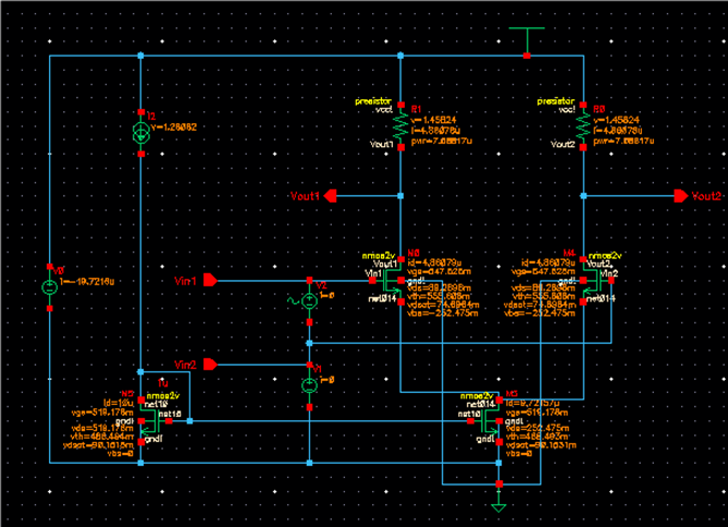
Figure 2. Common source level differential circuit topology.
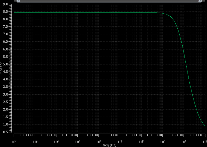
Figure 3. Ac gain of Common source level differential circuit.
2.2. Cascode
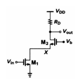
Figure 4. Cascode.
Fig.4 shows a cascode structure with resistance as the load.M1 is called the input device, the Vin is converted into a proportional current, M2 is a common source common gate device. The formula of its small signal model is derived as follows:
Av=gm1*gm2*Ro1*Ro2 (2)
In the cascode structure, the input signal is first amplified by the common source amplifier, and then further amplified by the common gate amplifier, and the voltage gain of the two amplifiers can be superimposed, thereby increasing the voltage gain of the whole circuit. By comparing the gain formula of single-stage amplifier, it is found that the structure of common source and common gate can achieve the effect of two-stage amplification. Next, need to connect a cascode circuit in Cadence. Because this paper needs to verify whether it can improve the circuit gain, it is necessary to control variables, that is, each pipe and circuit parameters remain unchanged, and to modify the basic common source differential amplifier circuit to obtain a cascode differential amplifier circuit. In Fig.2, Vin1 is the input voltage and Vin2 is the bias voltage, so Vin1 is connected to the gate end of M1. In Fig.5, due to the addition of first-level NMOS, M8 and M9 are connected to the input voltage of Vin1 as output terminals, and M0 and M4 are connected to the bias voltage of Vin2. The simulation results show that the circuit gain reaches about 23.
Comparing the circuit gain in Fig.3 and Fig.6, it can be found that the Cascode structure can indeed improve the gain of the circuit. Perhaps due to the influence of circuit parameters, the circuit gain is not very large, typically the gain of this structure is generally 20-30dB, which cannot meet the design requirements for high gain. Therefore, in practical applications, the gain is often enhanced by modifying the circuit structure. For example, changing to a cascode structure with a sleeve type can introduce external voltage bias to the gate terminal voltage of each stacked tube and increase the output impedance. This modification allows for a general gain range of 60-70dB. The folding cascode structure is more commonly used as it inherits the advantages of a large output impedance from the sleeve cascode structure while also increasing the output swing of the circuit. These characteristics enable the gain of folding cascode structures to easily exceed 70dB and improve noise suppression ability in power supply voltage. Additionally, it allows for self-compensation at the output end [5].
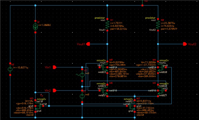
Figure 5. Cascode differential amplifier topology.
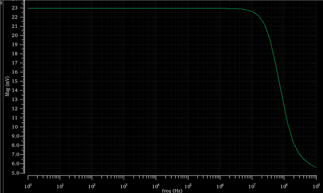
Figure 6. Ac gain of Cascode differential amplifier circuit.
This structure has both unique advantages and inevitable disadvantages. Firstly, the common-source common-gate structure has a high input impedance and low output impedance, which is beneficial for signal source matching and load matching, as well as improving the circuit's load capacity. Additionally, cascode structure exhibits good linearity, making it suitable for linear amplifier design. However, its main disadvantage lies in its high static power consumption due to both MOS being in a working state, resulting in large static power consumption for the cascode structure. Furthermore, it also suffers from poor thermal stability as the thermal effects of the two MOS affect each other, potentially leading to thermal stability issues.
2.3. Five-transistor OTA
In Fig 7, the five-transistor OTA contains the following five mos tubes: 1. The input pair constitutes the core differential amplifier of the OTA. 2. Use a pair of current mirrors as the load to increase the output impedance of the circuit. 3. Tail current source, which provides stable static bias current for the input pair.
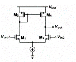
Figure 7. Five-transistor OTA.
Through the analysis of its small signal model, it can be obtained
\( Av=gm1,2*(Ro2//Ro4) \) (3)
In a five-transistor OTA in fig 8, a differential input signal is applied to the input end of the OTA, resulting in an increase in the gate-source voltage of one transistor in the differential pair and a decrease in the gate-source voltage of the other transistor. Due to the transconductance, the drain current of the differential pair transistor changes as a result of the change in the gate-source voltage. The current mirror replicates and amplifies the current change in the differential pair and feeds it to the common source amplifier at the output stage. Finally, the common-source amplifier converts the current into a voltage change, resulting in a proportional voltage signal at the output relative to the input voltage. To connect the circuit in Cadence, only need to remove the resistance load pair from the circuit in Fig.2 and use a pair of PMOS as loads to obtain a five-transistor OTA circuit. Keep all component parameters unchanged and perform AC simulation to achieve a gain of approximately 35.
Comparing Fig.3 and Fig.9, it is evident that the five-transistor OTA structure can also enhance the circuit gain. OTA stands for operational transconductance amplifier, and the five-transistor OTA is just one of the structures of OTA. In addition to the five-transistor OTA, there are numerous innovative structures being researched and applied in practical settings. For instance, a scholar developed an OTA EEG monitoring circuit based on the high efficiency, high precision and low power consumption of OTA combined with SG tunnel FET [6]. It presents a challenge to achieve low power consumption and high linearity of OTA under low power supply voltage using traditional low-power and linearization technologies. Another scholar proposed an OTA based on cross-coupled gate-driven quasi-floating MOSFETs and source level degradation linear technology [7], which effectively optimized the limitation of traditional OTAs. Furthermore, a telescopic cascade OTA was mentioned in literature as achieving higher output impedance and circuit gain compared to the five-transistor OTA [8].
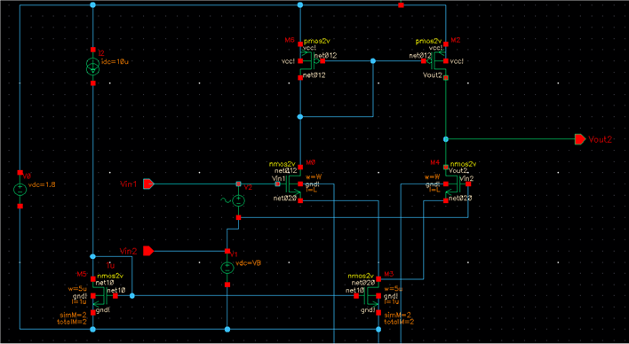
Figure 8. Five-transistor OTA circuit topology.
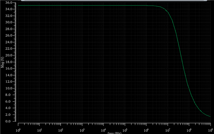
Figure 9. Ac gain of five-tube OTA circuit
The five-transistor OTA offers the advantages of simple structure, single-stage point, and suitability for low-voltage environment [9]. In addition, by adjusting the bias current and load resistance of the five-transistor OTA, various voltage gains can be achieved. This versatility allows for a wide range of applications in analog filters, analog multipliers and other circuits. However, like every coin has two sides, the five-transistor OTA also has some disadvantages. First of all, its linearity is poor due to limitations imposed by the linear working area of the MOS tube. As a result, it is prone to producing nonlinear distortion when handling large input signals. Secondly, the power consumption of the five-transistor OTA is relatively high, which may not be conducive to designing low-power circuits.
2.4. Cascade amplifier circuit
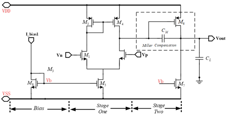
Figure 10. Cascade amplifier circuit.
The cascaded amplifying circuit is composed of multiple single-stage amplifying circuits arranged in a cascaded mode. In Fig.10 the circuit includes a current mirror as the differential stage of the load and a gain stage of a common source level structure that drives the CL load capacitor. In this amplifier, NMOS transistors M5, M7 and M8 are utilized to form a bias current source. Additionally, NMOS transistors M1,M2, and POMS transistors M3,M4 constitute a differential pair. Furthermore, PMOS transistor M6 and NMOS transistor M7 constitute a common source amplifier with current source as load. By analyzing its small signal model,
\( Av=gm1,2*(Ro2//Ro4)*gm5*(Ro5//Ro6) \) (4)
The formula demonstrated that the gain of the cascade amplifier circuit is equal to the product of the gain of each stage circuit. In line with the concept of controlling variables, the circuit depicted in Fig.10 is connected in Cadence software and its gain is approximately 52dB through simulation. Unlike the aforementioned circuits, it was observed that the gain of the circuit in Fig.11 was not readily apparent during ac simulation. Therefore, it is necessary to prompt a change to a closed loop for measuring its closed loop gain(stb simulation). During AC simulating, both positive and negative input terminals need to be connected to a DC voltage source to establish a common mode level.In addition,1V AC signal needs to be connected to the positive input terminal.In contrast, during stb simulation, the DC voltage source is connected to the positive input while setting the common mode level. What’s more, iprobe is used to connect the output to form a unit negative feedback loop.
A comparison between Fig.3 and Fig.12 reveals that the cascade amplifier circuit significantly enhances circuit gain.The form of cascade amplifier circuit also varies widely, not only the simple two single-stage amplifiers are cascaded together but they can also be combined with other types of amplifier circuit such as the five-transistor OTA and common source amplifier circuit mentioned earlier in order to create new amplifier circuits. The cascade circuit offers flexibility as several circuits or devices can be properly interconnected according to design goals so as to meet the specific requirements. Recognizing that limitations associated with individual Si IGBT or Sic MOSFET power devices restrict their application on their own, one scholar designed a cascaded H-bridge inverter by leveraging advantages such as low switching loss and high switching frequency from Sic MOSFETs along with cost-effectiveness from Si IGBTs [10].
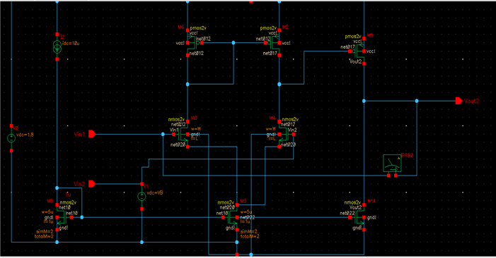
Figure 11. Topology of the cascade amplifier circuit.
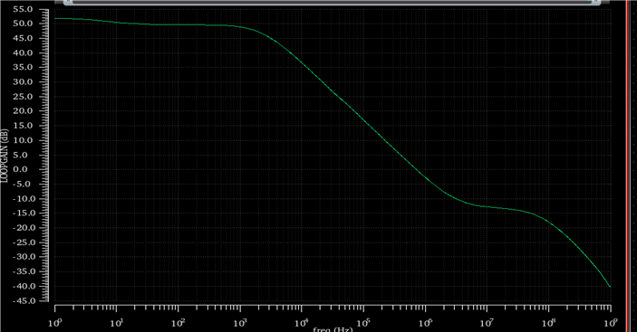
Figure 12. Gain of cascade amplifier circuit.
Like the circuits mentioned above, cascade amplifiers have both advantages and disadvantages. The most significant advantage of the cascade amplifier circuit is that it has a very high gain, as the gain of all levels of the amplifier circuit is superimposed on each other, resulting in a total gain that can reach a very high value. Secondly, the cascade amplifier circuit exhibits great linearity, effectively reducing signal distortion. This feather is particular important for fields such as audio and communication that require high signal quality. The cascade amplifier circuit offers flexibility by allowing combination with different single-stage amplifiers according to actual needs, making it adaptable to various application scenarios. However, the cascade amplifier circuit also has drawbacks, such as noise accumulation and complicated design. Noise in the cascade amplifier circuit mainly comes from the noise of the amplifier circuit at all levels. Due to the superposition of noise at all levels, the overall circuit may experience larger noise. Designing a cascade amplifier circuit is relatively complex as it requires consideration of matching, coupling mode, stability and other factors of the amplifier circuit at all levels. This complexity increases both difficulty and cost in designing the circuit.
3. Conclusion
This paper compares Cascode structure, five-transistor OTA structure, cascade amplifier structure and ordinary common source amplifier circuit through theoretical deduction and simulation to confirm their effect on gain. Moreover, through analysis of their respective advantages and disadvantages, it is found that each structure has its unique strengths but also unavoidable shortcomings. It is that each structure has its own strengths that make it possible to use different and more suitable structures in different applications.
Amplifiers, as a critical element within electronic circuit, inherently influence the overall system’s functionality. With the relentless progression of technology, the pursuit of amplifier gain optimization has emerged as a persistent research focus within the electronics domain. Beyond the limited advancements discussed in this paper, an array of innovative circuit tailored for various objectives has been developed. Furthermore, the novel semiconductor materials exhibit enhanced electron mobility and higher breakdown voltages, contributing to the augmentation of amplifier gain. As research into advanced semiconductor materials, such as graphene and gallium nitride, deepens, the realization of high-gain, low-power amplifiers is anticipated.