


1. Introduction
With the continuous advancement of technology, very large-scale integration (VLSI) has become one of the core technologies of modern electronic devices [1]. VLSI is an integrated circuit that integrates a large number of electronic components, including transistors, resistors and capacitors, which are integrated on a single chip to achieve various complex functions. The application scope of VLSI technology is very wide, including computers, communications, medical care, aerospace, and other fields. It has a high degree of integration, complexity, and importance. The application scope of VLSI technology is very wide, and it will play a more important role in various fields in the future. At the same time, the manufacturing process of VLSI technology will also continue to develop and improve to meet future needs and challenges. In short, VLSI technology will play a crucial role in future development. Integrated circuits are becoming more and more powerful, with higher integration and faster operating speeds, which have led to increasing power consumption of chips. To extend battery life, reduce cooling costs, improve device stability, and reduce environmental impact, it is particularly important to reduce chip power consumption. Therefore, when designing electronic devices, the importance of reducing chip power consumption should be fully considered.
2. Types of Power Consumption
Integrated circuits exhibit two distinct forms of power consumption: static and dynamic. Static power consumption arises when the circuit is energized but lacks potential inversion, while dynamic power consumption occurs during circuit operation, accounting for the power utilized during signal processing [2].
2.1. Static power consumption
Quiescent power is the amount of power generated by a circuit without logic conversion. It is mainly caused by leakage current inside the transistor, including gate leakage current, source leakage current, and drain leakage current. The higher the leakage current, the higher the quiescent power dissipation. In digital circuits, quiescent power dissipation mainly includes state hold power inside the transistor and quiescent power dissipation when the input transistor is on. Subthreshold leakage current is a tiny amount of leakage current between the source and drain when the gate voltage is lower than the threshold voltage that transistor need for linear turn-on.
 \( {I_{SUB}}=μ{C_{ox}}V_{th}^{2}\frac{W}{L}∙{e^{\frac{{V_{GS}}-{V_{t}}}{n}}}{V_{th}} \) (1)
W: channel width, L: channel length, \( {V_{th}} \) :thermal voltage, \( {V_{t}} \) :threshold voltage, n: a function of the device manufacturing process.
Gate leakage current is the current that passes through the gate oxide directly to the substrate. Drain leakage current is the current from the drain of the transistor to the substrate. There are several factors that affect the static power consumption of VLSI, which are Data transmission rate, Transfer mode, process size and Temperature.
The increase in data transmission rate means that more data needs to be transmitted per unit time, which will lead to an increase in the number of transistor switches and a corresponding increase in static power consumption Different transmission modes, such as parallel and serial, will directly affect the switching times and static power consumption of the transistor. For example, parallel transmission requires more transistors to work simultaneously, so quiescent power consumption is relatively high. As the process size decreases, the leakage current will increase, lead to an increase in static power consumption. As the temperature increases, the leakage current will also increase, resulting in an increase in static power consumption.
2.2. Dynamic power consumption
Dynamic power consumption in VLSI circuits stems from signal conversion and comprises primarily two components: switching and short-circuit power consumption [3]. Switching power consumption results from the transistor switch toggling on and off during signal conversion, while short-circuit power consumption arises from signal transmission short circuits. Additionally, there’s power consumption attributed to the charging and discharging of parasitic capacitors within the circuit.
The generation of dynamic power consumption is mainly related to signal conversion. In VLSI circuits, signals pass through a large number of logic gates and transmission gates during transmission, and the switching action of these gates causes changes in current, resulting in dynamic power dissipation. In addition, as the transistor size shrinks, so does the parasitic capacitance in the circuit, which also leads to an increase in dynamic power consumption [4].
Switching power consumption is the energy dissipated by the circuit during the switching process to charge and discharge the load capacitance of the output node.
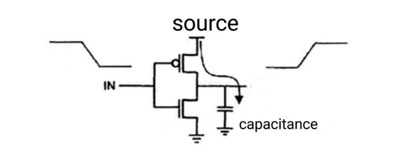
Figure 1. The cause of VLSI Switching power consumption.
The energy required for each flip of the load capacitor is
\( {\frac{Energy}{transition}=C_{L}}∙{Vdd^{2}} \) (2)
\( {C_{L}} \) is load capacitor, Vdd is power source. Switching power consumption is
\( Pydn=\frac{Energy}{transition}={C_{L}}∙{Vdd^{2}}∙{P_{trans}}∙{f_{clock}} \) (3)
Short circuit power consumption: Since the input signal is not an ideal square wave, it has a certain slope. Therefore, the input signal has a short time to make the NMOS and PMOS of the circuit turn on at the same time, so that the power supply of the circuit and the ground are short-circuited and the power dissipation caused by the circuit. The formula to count Short circuit power consumption is:
\( {P_{int}}=tsc∙Vdd∙{I_{peak}}∙{f_{clock}} \) (4)
tsc is the time of short circuit current, \( {I_{peak}} \) is all the current inside the circuit.
3. Ways to reduce VLSI power consumption
3.1. Transistor-level optimization techniques
The bottom layer of the logic gate-level optimization technology design process is only to the logic gate position, and the design tool completes the logic function and timing design of the chip based on the standard cell library [5]. The standard cell library contains various basic logic gates, such as NAND, NOR DFF, ADDER, MUX, etc., as well as some model parameters of each logic gate unit, such as power consumption, delay, drive capability, input, and output load, etc. There is also the layout shape, position, and so on of the logic gate unit. However, all logic gate units are ultimately implemented using transistors so that they can be produced on silicon. The same is the logic function of adder, and the topology of its transistor-level circuit can be varied [6]. The topology of the same adder, the selection of L and W values of the transistor, the layout of the layout, and the traces will also have a significant impact on performance and power consumption.
3.2. Gate-level optimization techniques
Gate-level low-power technology refers to changing some content in the circuit netlist through certain techniques to reduce quiescent power consumption and dynamic power consumption. The gate-level low-power technology that reduces dynamic power consumption is mainly the gate-level power optimization, including the optimization technology such as changing the drive capability of the device, switching logic port pins, phase allocation and buffer insertion [7]. For reducing quiescent power consumption, it is mainly by converting the device on the non-critical path from a low threshold voltage to a high threshold voltage device, reducing the leakage current, thereby reducing the quiescent power dissipation caused by the ground leakage current.
There are four ways Gate-level low-power technology to reduce dynamic power consumption: Changing drive capability is a way to reduce power consumption by changing the size of the unit device and thus the drive capability. For example, by reducing the drive capability of the logic gate, thereby reducing the size of the parasitic capacitance of its output node, or by increasing the drive capability of the logic gate to accelerate the conversion time of the logic gate output rise and fall, thereby reducing the short-circuit power consumption of the logic gate [8]. Another way to reduce power consumption is swapping the pins of the logic gate. It has been observed that the pin layout of logic gate elements in integrated circuit design libraries often exhibits a remarkable logical equivalence. For instance, three-input AND gates with three inputs and their pin-level equivalents can be effortlessly interchanged. However, it is worth noting that the parasitic capacitances of the input pins of these three-input AND gates may vary. It is therefore possible to lower the switching power consumption by arranging the wiring with a higher probability of transition to connect to pins with lower parasitic capacitances. The third way is to add inverters. If there is an inverter with a high flip rate in the design, we can reverse the signal by phase flipping, which not only reduces the area, but also reduces power consumption. Inserting buffer is also a good way to reduce power consumption [9]. If a logic gate driving capacity is small and its load capacitance is large, the conversion time of the output signal rising or falling will be longer, and the short-circuit power consumption of the next stage device will be relatively large. We can reduce the load capacitance by inserting buffers with moderate drive capability in the appropriate places. This not only reduces the conversion time of the device and improves latency, but also reduces power consumption.
Gate-level low-power technology to reduce quiescent power consumption: As device feature sizes continue to shrink and supply voltages decrease, the corresponding reduction in transistor threshold voltage is essential for ensuring performance. This adjustment is necessary because the leakage current’s power dissipation correlates inversely with the threshold voltage range, leading to a significant increase in leakage power consumption [10]. To mitigate the impact of leakage power dissipation, some semiconductor manufacturers provide libraries that encompass various threshold voltages: low, standard, and high. The control technology for device threshold voltages primarily achieves these levels—low, standard, and high—by managing the doping levels applied during fabrication. In relative terms, a device’s performance is inversely proportional to its leakage power dissipation; hence, a high-threshold voltage device will operate more slowly than a low-threshold voltage device but with reduced leakage power consumption [11].
3.3. System-level optimization techniques
System-level low-power technology is mainly from the perspective of the entire system, by optimizing the power consumption of the entire system and the individual modules in the system to reduce power consumption [12]. In general, the working mode of the system can be divided into normal operation mode and sleep mode. When the system is in sleep mode, some system-level low-power techniques can be employed, such as using a gated power method to cut off power and shut down inactive modules, which can significantly reduce the static power consumption of the system. The principle of gated power technology is to turn off the power of the chip’s unnecessary working area for a period of time, so that the power in other working areas continues to run. This approach can significantly reduce static power consumption throughout the design process, thereby extending battery life, which is important for wearable and portable mobile devices. However, the process of shutting down the power using gated power technology incurs additional power dissipation, which makes no sense if this power consumption is greater than the power savings using gated power technology. This low-power technology is only used if the power savings that can be achieved with this technology are much greater than the power consumption required for the power-down process. The implementation of this system-level low-power technology is also affected by various other complex factors.
In gated power technology, the way to shut down the power supply is generally divided into two types: off-chip shutdown and on-chip shutdown. Off-chip shutdown uses different power supplies in different areas of the general chip, and the power supply of some modules inside the chip is shut down through the regional power control port on the board level. On-chip shutdown refers to inserting a gated power switch unit into the power network inside the chip, and using this power control switch to turn off the power supply of some modules that are not working. Between the area where the power can be turned off and the area where the power has been powered, an isolation unit is usually used to isolate the two in order to prevent the influence of the always-on zone on the power-off area. Although the off-chip shutdown method can save more power consumption, the process of restoring power is quite slow, and the system performance cannot meet the designer’s requirements due to the poor stability performance of the external power supply.
4. Estimation of VLSI power consumption
There are three main methods for estimating power consumption: empirical estimation, simulation, and analysis. The empirical estimation method is mainly based on the designer’s previous experience and the power consumption data of similar circuits, which is subjective and uncertain. Two distinct approaches are commonly employed to assess circuit power consumption. The simulation method involves scrutinizing power consumption using dedicated simulation tools, offering relatively precise data but demanding substantial computing resources and time. In contrast, the analytical method entails estimating power consumption by constructing a circuit power model, enabling the acquisition of reasonably accurate data within a brief timeframe [13]. This analytical method has emerged as a focal point in contemporary research due to its efficiency.
The power estimation of integrated circuits is an indispensable part of the design process, and accurate power estimation can guide the optimal design of circuits to improve performance, reliability and energy saving. In the future, with the increasing scale and complexity of integrated circuits, power estimation methods and technologies will also face more challenges and opportunities. Research and development of more accurate, efficient and adaptive power estimation methods and technologies is of great significance to promote the development of integrated circuit design and manufacturing technology.
4.1. High-level power estimation
High-level power estimation is a method of evaluating the power consumption of electronic devices from a system-level or architecture-level perspective. It abstracts the logic and operational behavior of a system or circuit to create a simplified model that represents the actual operation situation. This model can provide detailed information about the system’s power distribution and trends, which can help with power optimization in the early design phase.
High-level power estimation is based on algorithms and statistical analysis. First, a high-level abstract representation is constructed by modeling the function and behavior of circuits and systems. This model is then used to predict power consumption under actual operating conditions through simulation or statistical analysis. This process typically involves selecting appropriate characteristics and parameters such as operating frequency, number of logic gates, and voltage.
introduction
With the increasing popularity of electronic devices, the issue of power consumption has also attracted increasing attention. For many devices, such as smart meters, IoT devices, and other embedded systems, low-level power estimation becomes particularly important. Accurately estimating the power consumption of these devices is important for optimizing system performance, extending battery life, and reducing operating costs. This article will deeply explore the technical principles, implementation methods, and application scenarios of low-level power estimation, and look forward to the future development trends.
4.2. Low-level power estimation
Low-level power estimation relies primarily on a deep understanding of hardware microarchitectures, including energy analysis of basic components such as processors, memory, and clock circuits. This analysis typically requires detailed modeling of the device’s hardware and taking into account dynamic factors such as the device’s workload, voltage, and frequency. Ideally, low-level power estimation also involves measuring the power consumption of individual operations or instructions. However, achieving such accuracy is often a challenge due to differences in hardware implementations from different vendors.
Achieving low-level power estimation often requires a range of techniques and tools. First, you need to collect detailed information about the hardware, including the specifications, operating parameters, and configuration of the hardware. This information can then be further leveraged to model the hardware’s power consumption by measuring the device’s energy consumption data. This process generally encompasses several stages, including data preprocessing, feature extraction, and model training. Ultimately, through the utilization of machine learning algorithms, it becomes feasible to forecast a device’s power consumption predicated on its operational condition.
5. Conclusion
The power consumption of VLSI is composed of phenomena caused by different causes, and the methods for reducing this power consumption are also different, and some of these methods are contradictory, reducing one type of power consumption while increasing another type of power consumption. Therefore, when using multiple methods simultaneously to reduce the power consumption of VLSI, it is necessary to consider the proportion of each power consumption and the benefits of each method to weigh the intensity of use of each method. This is a far more complex task than optimizing one-sided power consumption. Therefore, the method of evaluating power consumption is also crucial. Optimizing the power consumption of integrated circuits can bring a variety of benefits, including improved battery life, reduced energy costs, reduced device heat, and reduced environmental pollution. Under the combined effect of these factors, the development of human society will also go further. Therefore, this is an area worth investing in R&D and application.
Through the above research, the conclusion of this article is as follows: In VLSI, power consumption can be divided into dynamic power consumption and static power consumption. The methods for reducing these power consumptions can be divided into transistor-level optimization, gate-level optimization, and system-level optimization based on the operating scale, which correspond to improving the parameters of each transistor, changing the composition and connection of logic gates, and changing the entire system’s operating mode. In terms of power consumption estimation, it is mainly divided into high-level power consumption estimation and low-level power consumption estimation. Only by comprehensively considering all factors that generate power consumption and balancing the practicality of various power reduction methods, can a design that meets practical requirements and minimizes overall power consumption be achieved.