


1. Introduction
A switching power supply is a unique power supply that regulates the on-off time ratio of switching tubes to stabilize the output voltage. It was developed on the basis of the advancement of modern electronic power technology. Generally speaking, the switching power supply comprises of Pulse width modulation(PWM) control Integrated Circuit Chip(IC) and Metal-Oxide-Semiconductor Field-Effect Transistor(MOSFET). The switching power supply technology is continuously being improved upon as a result of advances in science and technology. The efficiency of switching power supply can be as high as 85%. Compared with ordinary linear power supply, the utilization efficiency of switching power supply is doubled. At the same time, the switching power supply adopts a small-sized filter element and radiator, which has high reliability and safety. According to the category of switching power supply, it can be divided into AC/AC (Alternating Current), DC/DC(Direct Current), etc. Among them, the converter of DC/DC switching power supply has achieved modular design and development, so it is generally recognized by users.
From the perspective of the emergence and development of switching power supply, since the 1960s, the emergence of thyristor control mode has greatly promoted the development of switching power supply. By the early 1970s, the switching power supply had entered a long bottleneck period, and the efficiency of the switching power supply became more prominent. Until the late 1970s, due to the innovation of integrated electrical technology, various switching power supply chips were born. At present, integrated power supply has been widely used in aerospace, color TV, computer and other fields [1].
This paper mainly discusses the current mode circuit, gives the difference between it and voltage mode, and studies the design idea and circuit of the A/D conversion circuit. Through the analysis of the current mode circuit, a 1bit A/D conversion circuit is designed by using the method of doubling circuit, comparing circuit and subtracting circuit. By comparing the series mode with the feedback mode, N bit A/D conversion circuit is designed. Through the analysis of the source of conversion error, the improvement measures are put forward, and the A/D conversion accuracy is improved. Through the discussion of this question, the diversified development of switching power supply control modes is promoted, which can have a certain influence on the switching power supply.
2. A/D converter
The A/D and D/A converters are important components in the power supply, among which, A/D converters are circuit modules that can convert analog quantities into digital quantities, and they are called analog-to-digital converters, or A/DC for short. Figure 1 shows a high-end A/D/DA analog-to-digital converter in lynx hilo, USA.
Figure 1. lynx hilo High-end ADC in USA
A/D converter converts analog quantity into digital quantity, which is convenient for single chip microcomputer to process data. Four procedures are often involved in A/D conversion: sampling, holding, quantization, and coding. In the actual circuit, various operations are integrated, such as sampling and holding, and the conversion process simultaneously implements quantization and coding. At the same time, the current mode circuit has the characteristics of high conversion speed, wide frequency bandwidth, low voltage and low power consumption. These characteristics can be fully utilized in A/D converters which are increasingly pursuing conversion speed and accuracy. This is also an important direction of A/D converter development [2].
2.1. A/D conversion concept
The circuit that converts analog signals into digital signals is called analog-to-digital converter (a/d converter or A/DC). The function of A/D conversion is to convert analog signals with continuous time and continuous amplitude into digital signals with discrete time and discrete amplitude.
A/D converter is divided into voltage mode circuit and current mode circuit. Its main technical indicators:
a. Resolution refers to the change of analog signal when the digital quantity changes by a minimum amount, which is defined as the ratio of full scale to the nth power of 2. Resolution, also known as precision, is usually expressed by the number of bits of a digital signal.
b. Conversion rate refers to the reciprocal of the time required to complete an A/D conversion from analog to digital. The conversion time of integral A/D is millisecond, which belongs to low-speed A/D, successive comparison A/D is microsecond, which belongs to medium-speed A/D, and full parallel/serial parallel A/D can reach nanosecond. Sampling time is another concept, which refers to the interval between two conversions. To ensure the correct completion of the conversion, the Sample Rate must be less than or equal to the conversion rate. Therefore, it is acceptable to equate the conversion rate with the sampling rate. Commonly used units are ksps and Msps, which represent thousands/millions of samples per second (kilo/Million Samples per Second).
c. Quantizing error: The error caused by the finite resolution of A/D, that is, the maximum deviation between the stepped transfer characteristic curve of finite resolution A/D and the transfer characteristic curve (straight line) of infinite resolution A/D (ideal A/D). Usually, it is the analog variation of 1 or half of the smallest digital quantity, expressed as 1LSB and 1/2LSB.
d. Offset error, When the input signal is zero, the output signal is not zero, and the external potentiometer can be adjusted to the minimum.
e. The difference between the corresponding input signal and the ideal input signal value when Full Scale Error is output.
f. Linearity The maximum deviation between the transfer function of the actual converter and the ideal straight line, excluding the above three errors.
2.2. A/D conversion principle
The current mode circuit realizes the A/D converter, and its design principle is shown in Figure 2, where Iref is the reference current and Iin is the input current, which is any value between 0 and Iref. After Iin is input, it is first doubled, and then compared with Iref. If 2Iin>Iref then the digital bit 1 is output. After subtracting 2Iin from Iref, it is fed back to the input to continue the above process. If 2Iin<Iref, the output digital quantity is 0, and 2Iin is fed back to the input to continue the comparison. The A/D conversion realized by this method has the same effect as the A/D converter of voltage comparison method, but the circuit is simpler [3].
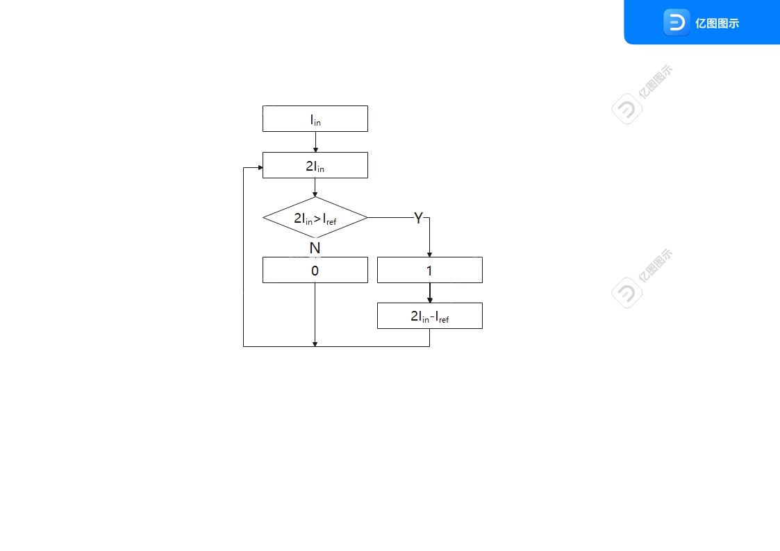
Figure 2. Schematic diagram of a/d conversion
2.3. A/D conversion steps
A/D conversion generally goes through four processes: sampling, holding, quantization and coding.
2.3.1 sampling and holding. Sampling is the process of periodically sampling the analog signal, that is, converting the signal that changes continuously with time into a series of pulses that are intermittent in time and equal in amplitude to the analog signal in the sampling time. In order to recover the original analog signal without distortion, the sampling frequency should not be less than twice the highest frequency in the input analog signal spectrum.
As the A/D conversion takes a certain amount of time to process, after each sampling, the sampled value should be kept unchanged for a period of time until the next sampling starts. This requires sampling and then entering the holding circuit. In the design, sampling and holding memory are in one circuit.
2.3.2 Quantization and coding. The sampled and memorized signal is still analog, not digital. It is the process of discretizing the output signal of the sample-and-hold circuit. The discretized signal is the quantized digital quantity, and the quantized digital quantity represented by binary is the code.
3. Circuit design and analysis of A/D converter
3.1. Circuit design of one-bit A/D converter
3.1.1 Design idea of one-bit A/D conversion. One-bit A/D conversion is composed of a doubling circuit, a comparison circuit and a subtraction circuit. The conversion circuit is composed of a MOS transistor and an operational amplifier. The current is doubled by a current mirror, the drain current is compared by an operational amplifier, the current value is judged, and then the high and low levels 1 and 0 are output.
3.1.2 One-bit A/D conversion design circuit. As shown in fig. 3, M1 to M9 are MOS transistors, and comp is a current comparator composed of operational amplifiers. M1 and M2 constitute a current mirror, and (W/L) [the aspect ratio of MOS pipe trench] in M2 is twice that of M1 (that is, 2:1). From the relationship between gate-source voltage VGs and drain current ID of MOS tube, it can be seen that the current of ID2 is twice that of ID1. M3, M4, M5 and M6, M7, M8 MOS tubes also constitute current mirrors, and their (W/L) ratio is the same, that is, 1:1:1.M9 is a gate switch. The working principle of the circuit is shown in Figure 3.
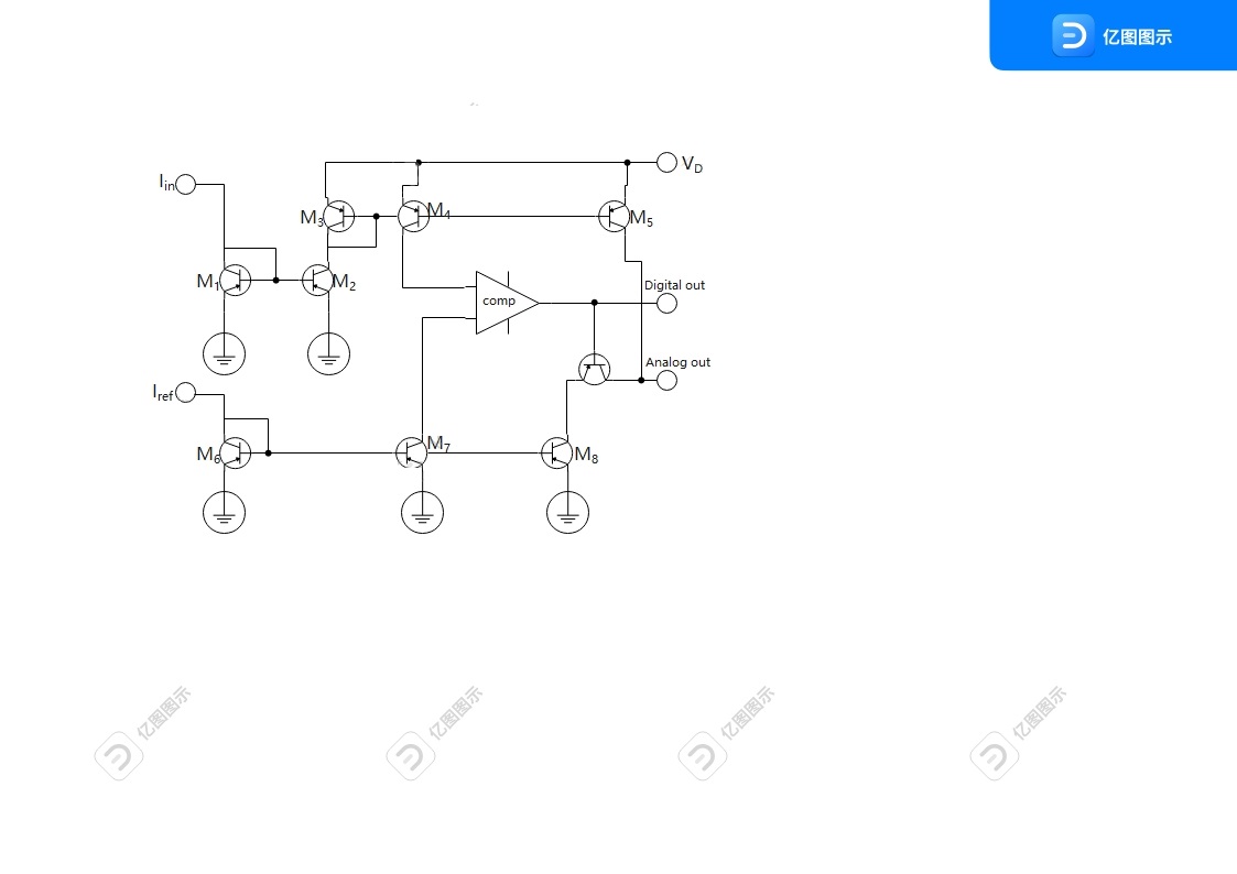
Figure 3. 1bit A/D converter circuit
The input current Iin is doubled to 2Iin through the current mirror formed by M1 and M2. Because M3, M4 and M5 are current mirrors, the drain output current of M4 and M5 is 2Iin. Iref flows through the current mirror composed of M6, M7 and M8, so the drain current of M7 and M8 is Iref. In this way, the drain currents (2Iin, Iref) of M4 and M7 are compared by the current comparator comp, and if 2Iin>Iref, the Digital output terminal digital outputs 1 level. At this time, the gate of M9 is at a high level, M9 is turned on, and the Analog output terminal Analog is (2Iin-Iref). If 2Iin<Iref, the array output is at 0 level, then M9 is turned off, and the analog output is 2Iin. At this time, the circuit realized 1-1bit analog-to-digital conversion[4-6].
3.2. Circuit design of multi-bit A/D converter
3.2.1 Design Ideas of Multi-bit A/D Conversion. There are two design ways to realize the A/D conversion of N bit. One is the serial mode, as shown in Figure 4. N 1-bit conversion circuits shown in Figure 3 are cascaded. The analog output of the previous stage is used as the analog input of the next stage, and the digital signals are output in parallel. The N bit converter realized in this way needs N 1-bit unit circuits as shown in Figure 3, and does not need control signals. Moreover, the digital signals are output in parallel, and the conversion speed is high, but it requires more hardware. The other way is feedback, which feeds the analog output signal back to the input, and the auxiliary circuit realizes N bit conversion. This second way is adopted in this paper.
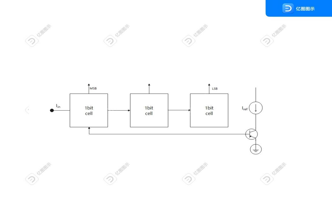
Figure 4. Design principle of series N bit A/D converter
3.2.2 Design circuit of multi-bit A/D conversion. As shown in Figure 5, the feedback mode consists of M1~M9 1bit A/D unit circuits, M10~M13 and M14~M17 memory circuits and S1~S4 timing control switches. The working sequence pulse waveform of the circuit is φ1~φ4, as shown in Figure 6.
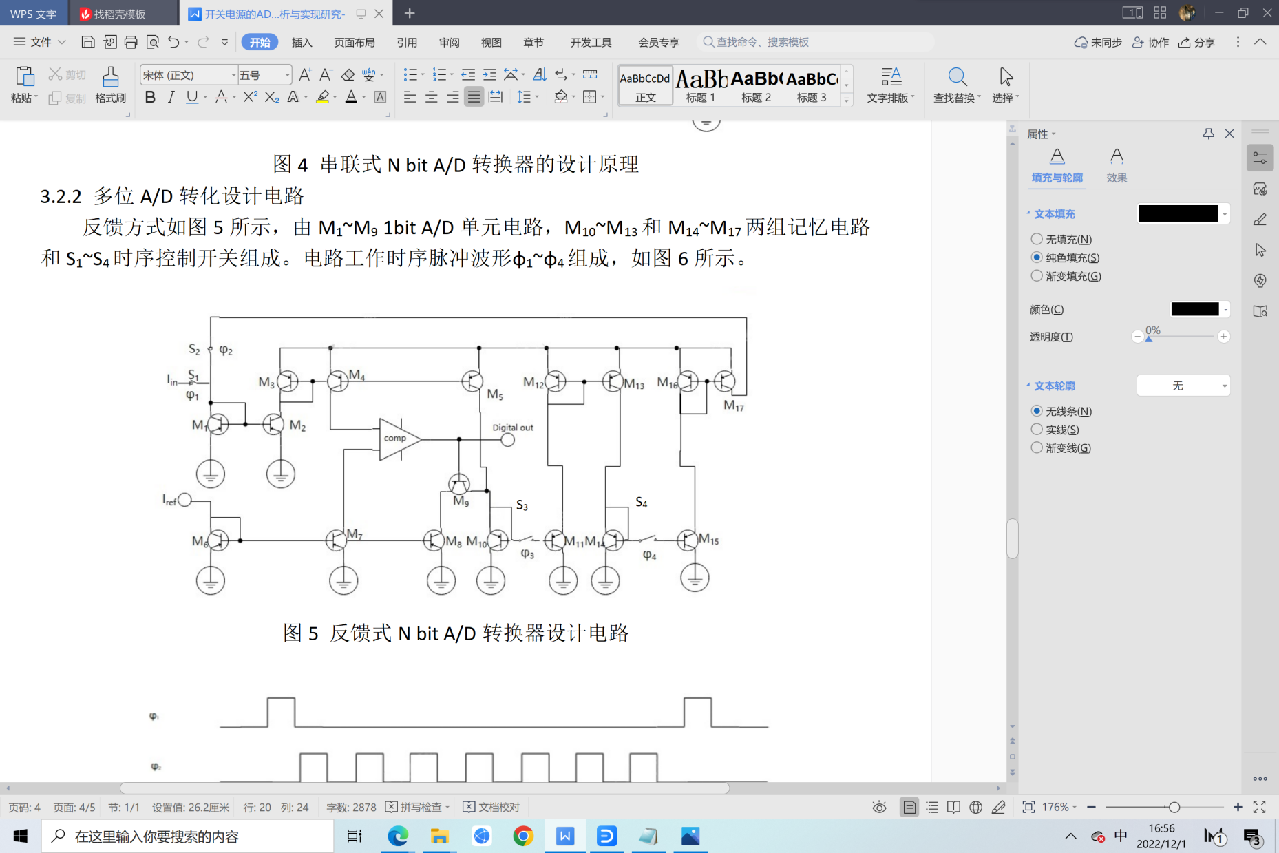
Figure 5. Design circuit of feedback N bit A/D converter
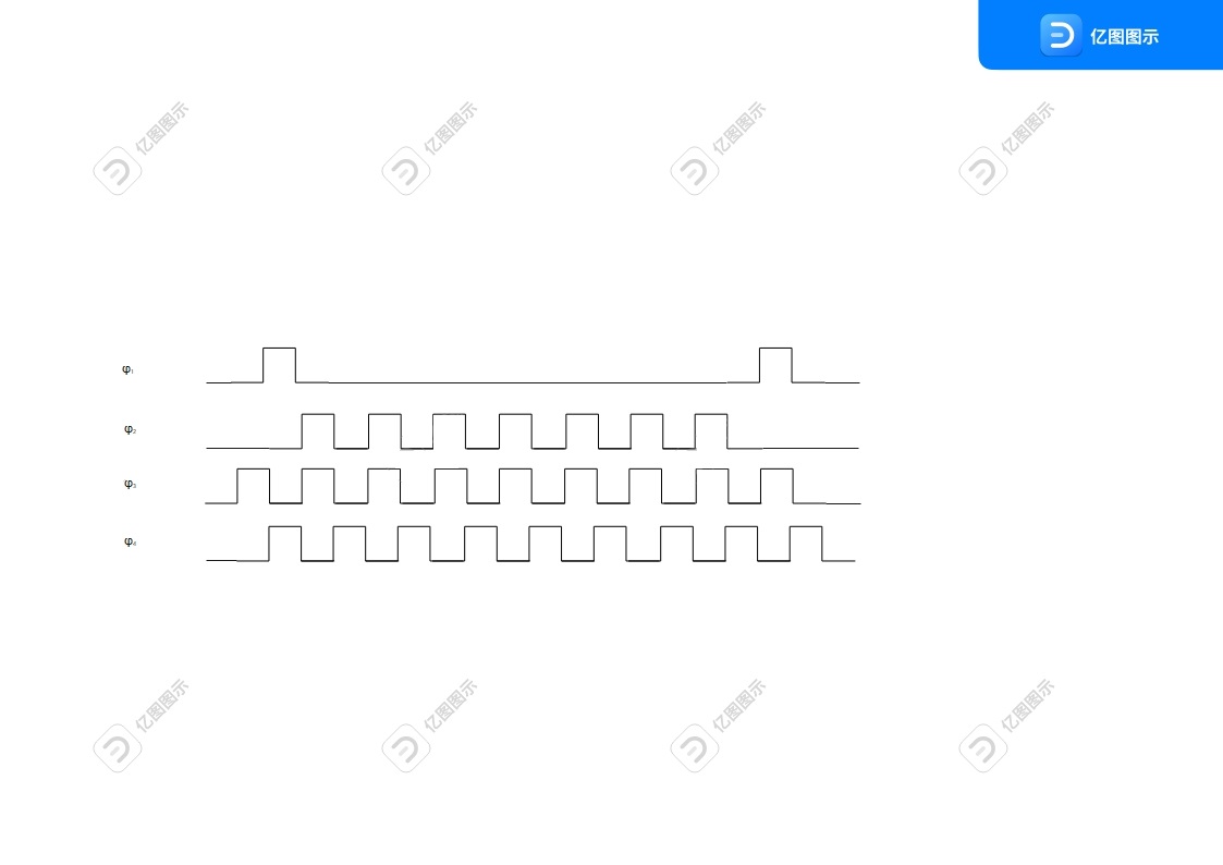
Figure 6. Timing pulse waveform of feedback N bit A/D converter
When the circuit starts to work, assume that the circuit is in the period of n-1 pulses. At this time, φ1(n-1),φ3(n-1), the level is 1, φ2(n-1),φ4(n-1), and the level is 0. S1, S3 are closed, S2,S4 are open. The input current Iin is converted by 1bit, and the first digital signal is output, which is the highest bit Dn-1. The converted analog output charges the gate-source capacitors of M10 and M11. When φ1 (n), φ3 (n), φ2 (n) are at 0 level and φ4 (n) is at 1 level, S1, S2 and S3 are off and S4 is closed, the analog output after the first conversion is kept on the gate-source capacitance of M11 in the memory cells M10~M13. Because S4 is closed, the analog quantity in the memory cells M10~M13 is transferred to the memory cell M14. Start the second bit conversion. At this time, φ1 (n+1), φ4 (n+1) are at 0 level, φ2 (n) φ3 (n) is at 1 level, S1 and S4 are turned off, and S2 and S3 are closed. At this time, the analog quantity after the first conversion held in M14~M17 memory cells is used as the input analog quantity 1-bit conversion circuit through the switch S2, and the second A/D conversion is carried out to output the second digital signal Dn-2, and the process is repeated until the N bit digital signal is output. The digital signal output by feedback mode outputs the high bits first and then the low bits. Although the conversion speed is not as good as that of series mode, it saves a lot of hardware circuits[4-6].
3.3. A/D converter error problem solving method
3.3.1 A/D Error of A/D converter. The accuracy of A/D converter is mainly affected by the degree of current mirror's absence and the accuracy of current transmission between current mirrors. When the current mirror is not strictly matched, that is, ΔI=Iout-Iin≠0, the current error ΔI is:
 (1)
(1)
In which Δg is the difference of transconductance G of two MOS transistors, ΔT is the difference of turn-on voltage of MOS transistors, and g is defined as  ,
, is defined as mobility,
 is defined as the gate-source capacitance. When Δg=0,
 (2)
(2)
That is, the current error is proportional to the square root of the input current.
When ΔVT=0,
 (3)
(3)
That is, the current error is proportional to the input current. Generally, Δg and ΔVT can be close to 0.2%.
3.3.2 Solutions. The current transmission error between mirrors is mainly caused by the limited input and output resistance of MOS tubes, which can be expressed as:
 (4)
(4)
I01, r01 are the output current and output resistance of M1 current mirror, and Iin, 1/gm2 are the input current and input resistance of M2 current mirror. It can be seen from the formula (4) that if the current transmission accuracy is to be improved, i.e., Iin2/I01 should be close to 1, i.e., r01 should be increased or 1/gm2 should be decreased. The use of a current mirror can improve the transmission accuracy of current[4,6].
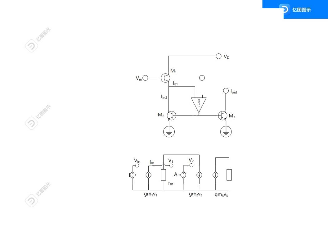
Figure 7. Active current mirror circuit and equivalent circuit
As shown in fig. 7, an operational amplifier is added between the drain and the gate of the current mirror M2. As can be seen from Figure 7:
 (5)
(5)
 (6)
(6)
 (7)
(7)
From the formulas (5), (6) and (7), we can get:
 (8)
(8)
Where A is the closed-loop amplification factor of the operational amplifier, which can be obtained from formula (8):
 (9)
(9)
Due to Agm2r01»1, the formula (9) can be simplified as:
 (10)
(10)
It can be obtained from formula (10) that if the active power mirror replaces the basic power mirror, the current transmission accuracy can be improved by two orders of magnitude. For example, taking the typical values of r01 and gm2: r01=5MΩ, gm2=20μA/V, for the basic current mirror (that is, A=1), you can get:
 (11)
(11)
For active current mirror A=100, we get:
 (12)
(12)
4. Conclusion
This paper discusses the design idea of current mode, designs 1-1bit and NbitA/Dz conversion circuits, studies the conversion error and gives the solutions. It can be concluded that the current mode of switching power supply is used to realize A/D conversion, so the circuit is relatively simple, the power consumption is small, and the analog-to-digital conversion speed is fast. The active current mirror can greatly improve the A/D conversion accuracy. Using current control mode to realize A/D conversion is worthy of further discussion in response characteristics, loop stability, high-frequency power loss and overload protection. Miniaturization and high-frequency A/D conversion have become the development trend, and the application of digital control technology is also the focus of current research.