

1. Introduction
Over the last few decades, thermal flow sensors have become indispensable in various industrial and research applications. These sensors are commonly categorized into three primary types: hot wire/hot film flow sensors (by detecting changes in resistance caused by fluid cooling of a heated element), calorimetric flow sensors (by measuring changes in heat carried by the fluid), and thermal time-of-flight (TOF) flow sensors (by measuring the time it takes for a thermal pulse to travel through the fluid).
The development of thermal flow sensors began with the hot wire anemometer in the 1910s [1], then hot film anemometers in the 1950s [2], calorimetric flow sensors in the 1970s [3], and thermal TOF flow sensors in the 1980s and 1990s [4] approximately. A significant transformation occurred from the late 1980s to the mid-1990s with the development of Micro-Electro-Mechanical Systems (MEMS) technology [5-7], leading to a wide use [8-12]. At the same time, CMOS technology also upgraded [13-15]. These improvements contribute a lot to the research of CMOS-MEMS thermal flow sensors.
There are few MEMS thermal flow sensors integrating their CMOS readout within a single package to create CMOS-MEMS thermal flow sensors, thus deserving further discussion [16]. However, resent research has shown that CMOS-MEMS technology significantly enhances sensor performance [16-19]. This is particularly beneficial for applications in areas such as heating, ventilation, and air conditioning (HVAC) [20]-[22], medical devices [23]-[25], and industrial process control [16,26,27].
Although significant progress has been made, current research focus on expanding applications and improving existing technologies. It is true that the advantages like reduced size and weight and improved power efficiency can be seen as huge achievements, however, limitations including limited material choice and inaccuracy due to heat lost also made it a long way to ultimately widely use these CMOS-MEMS thermal flow sensors in the industrial field. Future developments are likely to focus on further enhancing the integration of CMOS-MEMS technology. All of these will be fully discussed later.
In the subsequent content, the authors will analyse the principle of CMOS-MEMS thermal flow sensors, listing advantages and limitations. Based on this, the application fields will be presented in detail. Finally, this paper will conclude with outlining possible future development prospects.
2. Advantage and limitaion of cmos-mems flow sensor
2.1. Principle of CMOS-MEMS technology
2.1.1. Pre-CMOS MEMS
It is universally acknowledged that the modular integration process, originally invented at Sandia National Laboratories (SNL), serves as the representation of pre-CMOS technologies [28].
As the name implies, in pre-CMOS technology, MEMS structures are predesigned and embedded in silicon wafer, which is subsequently filled with oxide or dielectrics. Following this, the wafer undergoes planarization to prepare it for subsequent CMOS electronics processing steps. This "MEMS-first" approach, despite the predefined nature of the MEMS structures, necessitates a wet etching process after the completion of standard CMOS procedures to liberate the pre-formed MEMS structures.The intricate fabrication of pre-CMOS MEMS Thermal Flow Sensors necessitates a photolithography step for meticulously patterning the MEMS features within recessed structures. Consequently, the achievable thickness of these MEMS constructs is inherently circumscribed by the photolithographic limitations, particularly the focal depth capacity, which determines the precision and resolution at which patterns can be faithfully transferred onto the substrate. To address this constraint, advanced lithography techniques, such as multi-layer exposure strategies or the employment of specialized lenses with enhanced depth of focus, are being explored and adopted to enable the realization of thicker yet high-precision MEMS layers, thereby broadening the design horizon for CMOS-integrated thermal flow sensors.
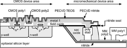
Figure 1: Schematic cross-section of pre-CMOS MEMS processes for fabrication of monolithically integrated polysilicon microstructures from SANDIA M3EMS) [29]
2.1.2. Inter-CMOS MEMS
Inter-CMOS MEMS is a technology where CMOS processing stages are intertwined with with additional processes of polysilicon thin film deposition and micro-machining to construct sensor structures. During wafer manufacturing, the deposition and release of sensor polysilicon thin films are alternated with contact formation and metallization in the adjacent CMOS circuitry, a methodology that has been extended to encompass SOI CMOS MEMS products. Infineon, another prominent player in automotive sensor technology, employs the inter-CMOS methodology to produce its integrated capacitive pressure sensors. This series of integrated sensors remains in high-volume production and finds widespread application in smart tire pressure monitoring systems (STPM) [30] as well as in manifold absolute pressure measurements within automobiles.
2.1.3. Post-CMOS MEMS
In contrast to the previous two approaches, post-CMOS MEMS involves executing all MEMS processing steps subsequent to the full completion of CMOS fabrication. Depending on how the MEMS structures are formed the CMOS circuitry, post-CMOS MEMS technologies can be classified into two main categories: additive and subtractive to the CMOS. In the additive post-CMOS MEMS, structural materials such as AlN [31] are deposited directly onto the CMOS substrate. Conversely, subtractive post-CMOS MEMS involves selectively etching CMOS layers, including the substrate to create MEMS structures. This can be achieved through two methods: a precisely timed backside etches with a calibrated etching rate, or utilizing an automatic etch stop technique to form silicon membranes or MEMS structures [32].
For instance, the fabrication of MEMS resonators integrates the surface micro-machining process of cantilever fabrication with the traditional CMOS process. In this scenario, the release of the MEMS structure takes place subsequent to the CMOS process, which includes additional steps such as selectively removing the silicon nitride capping layer prior to MEMS annealing for stress management and applying a photoresist coating for protection [33].
2.2. Advantages of CMOS-MEMS thermal flow sensors
CMOS-MEMS technology enables the integration of multiple components and functionalities onto a single chip, thereby enhancing the sensor's compactness, efficiency, and reliability. This high integration level offers several benefits:
2.2.1. Reduced size and weight
CMOS-MEMS combination integrates sensor elements, control circuits and signal processing units on a single chip, which results in a rather smaller sensor package. The study in IEEE Sensors Journal, 2017 demonstrates an integrated CMOS-MEMS flow sensor that senses nitrogen flow ranging from 0 to 26 m/s within a very compact system-on-chip (SoC) [34]. This high level of integration not only reduces the sensor's volume, but also minimizes its weight. This indicates that the CMOS-MEMS technology has a wider range of application prospects, that kind of thermal flow sensor can work in space-constrained environment.
2.2.2. Improved power efficiency
The complementary NMOS and PMOS transistors in CMOS technology determines low static power dissipation, so CMOS-MEMS combination inherently improve power efficiency. For instance, the thermal isolation of gas sensing through post-CMOS MEMS technology in the fabrication of Chemo-resistive type gas sensor makes a noticeable improvement on the capability of forming monolithic sensing systems. [35]
2.2.3. Enhanced functionality
Profited from the integration of multiple transistors and other electronic components within a single chip, CMOS-MEMS thermal flow sensor could realize advanced sensing and control systems that can perform multiple tasks simultaneously, and the integration of heaters, temperature sensors, signal conditioning circuits and microcontrollers allows for precise flow measurement [36]. Obviously, the functionality of the sensor is enhanced driven by CMOS-MEMS combination.
2.2.4. Increased reliability
The reduction of interconnections in circuitry minimizes the risk of failures due to wear and tear or environmental factors. Additionally, delicate circuit design ensures higher quality and consistency during manufacturing process [37]. Cai’s team detected resistance to environmental factors such as temperature, humidity and mechanical stress, as well as stability during long-term use based on thermal flow sensors, then come to the conclusion that this integration does increase reliability [38].
2.3. Limitations of CMOS-MEMS thermal flow sensors
Despite all the benefits that CMOS-MEMS integration technology brings, it also has some problems such as the limited material choice and inaccuracy caused by heat loss. This section will address these main problems and aim to inspire readers’ thoughts. This section lists the main limitations of CMOS-MEMS thermal flow sensors and discusses existing solutions for these issues. However, these solutions often involve trade-offs. While they address some major limitations, they also introduce new challenges, such as increased complexity in the manufacturing process.
2.3.1. Limited material choice
Typically, the CMOS-MEMS fabrication methods are based on post-CMOS technology, subtractive manufacturing method are preferred. Post-CMOS technology requires careful handling to avoid damaging the CMOS structure during MEMS device fabrication. Therefore, manufacturers must ensure that processing temperatures do not excess 400℃ [26,39]-[41] and meet other stringent conditions. Such strict environment requirements limit the materials available for making CMOS-MEMS structures to only polysilicon and metals. As a result, some kind of material like ceramic, a good choice to make thermistors [42]-[44] in thermal flow sensor, cannot be fabricate due to material limitation. This limitation results in a lack of diversity in CMOS-MEMS thermal flow sensor designs.
Recently, Roy's team successfully deposited carbon nanotubes (CNT) on CMOS during the CMOS-MEMS process [45] (as shown in Figure 2). They first built a heater on the CMOS, which can heat the local temperature on the CMOS to around 650-800 ℃ without damaging the CMOS structure. In this temperature range carbon nanotubes can be synthesized. It providing an idea for how to fabricate other materials with high annealed temperature to prepare thermal flow sensor in the CMOS-MEMS fabrication process.
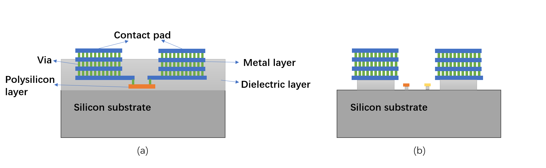
Figure 2: Concept diagram of Li's team preparing carbon nanotubes on CMOS chips. (a) Schematic cross-section viewed from x direction. (b) Schematic cross-section viewed from y direction
However, this method adds too many steps in processing. How to find a simpler solution is still what we need to think.
2.3.2. Inaccuracy due to heat loss
In CMOS-MEMS integrated sensors, most of the MEMS devices are fabricated on the CMOS. However, for thermal flow sensors, this integration approach can inadvertently cause the dissipation of heat generated by the heater along the interconnecting pathways. This will lead to inaccurate of measurement. Therefore, reducing the conductive heat loss is important [46].
Implementing thermal isolation for MEMS devices integrated with CMOS substrates is a widely adopted solution to address the heat dissipation in thermal flow sensors. Currently one primary method is employed for achieving effective thermal isolation, using low thermal conductivity(𝑘) substrate materials [46].
The commonly used low thermal conductivity materials are ceramics or polymers (as shown in Table 1). Ceramics such as glass (𝑘 = 1.1 W/(m·K) [47]), porous silicon (𝑘 = 1.2 W/(m·K)[48]) and aluminium oxide (𝑘 = 20 W/(m·K)[49]). While, the thermal conductivity of polymers is generally lower. Polyimide (𝑘 = 0.29 W/(m·K)) has been widely use as substrate material [50]-[52]. By incorporating these materials into the design, the transfer of heat from the heater to the surrounding CMOS substrate is significantly reduced.
Table 1: Thermal conductivity of different materials
Material | Thermal Conductivity(W/m·k) |
Silicon | 130 |
Glass | 1.1 |
Porous Silicon | 1.2 |
Aluminum Oxide | 20 |
Polyimide | 0.29 |
Another effective solution is to hang MEMS device. By using deep reactive-ion etching (DRIE) hollowing the bottom part out of already generated MEMS devices [17,53,54]. The commonly used method is etching substate with XeF2 [17,20,21,53] (as shown in Figure 3). By hanging the MEMS part with only remaining thin metal bar above, it can be ensured that its heat will not be greatly lost due to it isn’t contact with CMOS substrate. Thus, avoid the heat loss problem of thermal flow sensors.
Figure 3: Post-CMOS process for the release of the CMOS thermal flow sensor microstructure by using XeF2
2.3.3. Increased processing complexity
From the above two defects, it can be seen that in order to manufacture CMOS-MEMS integrated chips, the manufacturing process is more complex than using CMOS and thermal flow sensors individually. Because it not only requires basic MEMS manufacturing, but also ensures the integrity of the CMOS structure. This leads to many etching and deposition steps that are unrelated to the structure of the thermal flow sensor itself. In order to prevent etching and other behaviours from damaging the CMOS structure, precise time and quantity control of MEMS manufacturing steps is often required, which further increases the complexity of manufacturing.
Moreover, in order to solve temperature drift, thermal flow sensors sometimes require the additional compensation resistors in the circuit [55]. The excess device manufacturing also increases the complexity of the overall manufacturing process of CMOS-MEMS thermal flow sensors.
At present, the majority of CMOS-MEMS manufacturing relies on CMOS foundries providing CMOS substrates, and then manufacturers processing MEMS devices on them. Most CMOS substrates provided CMOS chips separately. Which means they are not in wafer. This leads to a very complex manufacturing process for thermal flow sensors on CMOS.
2.3.4. High cost of time and money
As mentioned earlier, the CMOS-MEMS process is complex, resulting in the use of more materials and processes in the manufacturing section, which means more cost [26],56]. At the same time, CMOS substrate is provided by CMOS foundries. Due to the fact that the CMOS chips provided by CMOS foundries are individually separated, a significant amount of time and experience are required during the MEMS processing stage. If the MEMS to be manufactured is much larger than CMOS, it will require even more expenses [57]. Therefore, currently, CMOS-MEMS manufacturing has high time and monetary costs. This problem may only be solved when CMOS-MEMS technology matures and forms standards one day.
3. Application
Nowadays, researchers dig into expanding the range of CMOS-MEMS thermal flow sensors. Some representative fields can be HVAC, medical and industrial field.
3.1. HVAC field
Due to the powerful airflow measurement abilities, CMOS-MEMS thermal flow sensors are considered a promising choice for the HVAC area. As previously mentioned, several results have been reported by different teams. For instance, a team led by Wei Xu and Xiaoyi Wang introduced a bidirectional thermosensitive microcalorimeter (TMCF) sensor realized through 0.18μm CMOS-MEMS technology. This sensor achieved a maximum sensitivity of 453 mV/(m/s) within a bidirectional airflow velocity range of -6 to 6 m/s (with a signal amplification gain of 250 and input heating power of 1.58-1.72 mW, the highest normalized sensitivity was 1150 mV/(m/s)). Also, this flow sensor can accurately measure indoor airflow even at very low speeds (<0.05 m/s). These characteristics make the sensor a promising candidate for airflow sensing nodes in HVAC systems and potentially for counting the number of people in buildings and rooms. Indeed, given the direct release process of MEMS, this sensor is well-suited for large-scale production using CMOS technology, offering a cost-effective multi-sensor node monitoring solution for intelligent HVAC systems and other industrial applications [20].
Particularly in large buildings, to achieve better effects, a HVAC System is needed. Zhaoliang Liu reported an energy saving monitoring network of building central air conditioning based on physical sensor network technology. The system can collect on-site operation parameters and transmit them to the upper computer of the monitoring center through GPRS network to realize the energy-saving management and optimal control of the whole system. [58]
3.2. Medical field
Carbon dioxide is a critical gas for humans, and there is an urgent need for CO2 detection devices in the medical field. However, we find microcantilever sensors better studied in this field. For example, A. Mirza and his team introduced a CMOS-MEMS microcantilever sensor designed specifically for CO2 measurement applications. They conducted sensitivity analysis on sensors with different polymer coating thicknesses. The results indicated that the shift in resonant frequency increased with the thickening of the polymer layer. With a polymer layer thickness of 5μm, the sensor's sensitivity was 3.18 Hz/0.01%V or 3.18 Hz/100ppm. Compared to traditional infrared analysers and mass spectrometers, this sensor offers advantages such as low cost, low power consumption, ease of calibration, and portability. Therefore, this CMOS-MEMS microcantilever sensor is particularly suitable for home healthcare and clinical services [25]. We also learned that other researchers are trying to develop CMOS-MEMS thermal flow sensors. They have better performance for detecting CO2. We will keep on following up and reporting on their progress.
It is worth noting that in the medical field, other CMOS-MEMS devices exist besides CMOS-MEMS thermal flow sensors. For example, the medical resonator reported by A. A. S. Rabih's team can detect acetone in exhaled breath for diagnosing diabetes. This device also features miniaturization and low cost [24].
3.3. Industrial field
In today's industrial processes, especially in chemical plants, thermal flow sensors are of great importance. Traditional sensors have many shortcomings, including high cost, large size, and complex operation. Therefore, alternative solutions are necessary. M. Ahmed and his team reported the CMOS-MEMS thermal flow sensor that we mentioned earlier. This integrated CMOS-MEMS flow sensor utilizes More-than-Moore technology to detect bidirectional N2 gas flow. Based on sensitivity measurements (98 mV/sccm, which is three times the state-of-the-art) and SoC measurements of flow rates ranging from -26 to 26 m/s (-50 to 50 sccm), this sensor is exceptional. Additionally, due to its pulsed heater operation, the flow sensor exhibits very low power consumption (<9 mW). It is anticipated to be an excellent candidate for applications in smart homes and industrial processes.
Apart from that, Y.-C. Lee and his team reported a kind of CMOS-MEMS optical-based gas sensor. It also plays a big role in the oxygen and carbon dioxide measurement [59].
In addition to the work mentioned above, there are other sensors in the invention method. Overall, CMOS-MEMS thermal flow sensors are a good choice for a wide range of fields due to their low cost, portability, and high flexibility. The ongoing exploration and subsequent reporting of sensor technologies will be pursued diligently.
Additionally, other CMOS-MEMS devices will be good alternatives for old devices. It is expected that more CMOS-MEMS thermal flow sensors and different kinds of CMOS-MEMS devices will be introduced in this field in the future.
4. Conclusion
This article looks closely at CMOS-MEMS thermal flow sensors. It explains how they work, the kinds there are, and how they've gotten better with CMOS technology. It talks about the good things about this technology, like how it makes things fit together better, costs less, and uses energy more wisely. It also points out some problems, like the materials not being perfect, not being able to measure heat loss exactly, and making the process of making them more difficult. The article also looks at how these sensors can be used in heating and cooling systems, medical equipment, and controlling how things work in factories.
By examining at the review and other related literature, this paper shows how CMOS-MEMS thermal flow sensors can be used in the future. It talks about how they can work with many parts together and handle very hot or very cold temperatures. This shows that this technology has a good future and can help many areas grow.
4.1. Multi-module integration
Multi-module integration is a way to design software systems. It divides a large, complicated software system into smaller parts. Each part does a specific job. These parts don't mix with each other but they work together using clear rules and ways to communicate. In CMOS-MEMS technology, this is used to put microelectronics together with tiny machines. This makes very small systems that are packed closely together. [60,61].
Multi-module integration provides great support for the development of CMOS-MEMS sensors. It makes the sensors' measurements better because it puts different parts that do different things on one chip. This means there are fewer connections outside the chip, which helps the signals stay strong and clear [20,62]. It also makes the signals better by reducing extra effects and problems [19,63]. Since the signals don't have to travel far, the sensors can react faster and work quicker [60,63]. Plus, it helps the sensors that measure heat, like the ones with thermistors, to be more accurate because it uses less energy and makes less heat [16,20,64,65]. Using less energy also means less heat is made [19,20,46]. Better designs for managing heat and shorter paths for heat to travel also help the sensors work better [17,19,64]. Multi-module integration also makes the sensors smaller and lets us design them in more ways [62].
But multi-module integration in CMOS-MEMS thermal flow sensors faces challenges due to technical complexities like signal interference, thermal issues, and intricate manufacturing [16,20,66]. Even though it might cost less to make each sensor, the high costs at the beginning can stop people from using it, especially if they don't see all the good things, it can do yet. People might still like the old sensors that only do one thing and might be worried about the risks and costs of using new technology, which can also stop this integration technology from being used a lot.
4.2. Extreme temperature
As technology advances, it's more possible for future flow sensors to work in very tough places like the North and South Poles and space. These places have extremely hot or cold temperatures and big changes in pressure, which make it hard for sensors to work well. So, making flow sensors that can measure things very accurately in these tough conditions is getting more important. We need to make the sensor materials stronger and design them better so they aren't affected by the environment. Making sure sensors work right in extreme temperatures is very important for science and exploring new places.
Existing CMOS-MEMS thermal flow sensors face three main issues under extreme temperature conditions:
Material Selection Limitations: The materials that work with CMOS might not be good for very hot temperatures [67]. This means there aren't many materials to choose from. Some materials that can handle high temperatures, like PDCs, silicon-sapphire, silicon-diamond, 4H-SiC [20,36,64], are hard to design and package for sensors as they are also costly [68]. Also, when the materials change, it can make the sensors react slower and not be as sensitive [69,70].
Manufacturing Process Challenges: Using special materials means a need of better and more expert ways to make them. For example, some materials that can handle high heat might require more special processes to engraving or layering processes. [26,71]. Also, packaging technology is also a key aspect of the manufacturing process. e need to make sure the sensor can exchange heat well with the outside while keeping the electronic parts safe from harm. This mix of needs for packaging makes it harder to seal the sensor properly [72].
Influence of High-Temperature Environment: Under high-temperature environments, affected by thermal stress and expansion [73,74], the sensitivity of CMOS-MEMS thermal flow sensors may decline, specifically in aspects such as high-temperature response time of the sensors. At the same time, accelerated degradation tests indicate that under extreme conditions, the signal processing system (SPS) of CMOS-MEMS flow sensors is prone to attenuation [74,75], thereby affecting the stability and durability of the sensors.
Of course, with the advancement of technology, there are increasingly more successful cases of CMOS-MEMS thermal flow sensors that can cope with extreme environments [76,77]. In general, future research on CMOS-MEMS thermal flow sensors for extreme environments can focus on optimizing manufacturing processes and exploring new materials and technologies.
Acknowledgement
Ang Li, Haonan Zhao, Yufei Zhou and Zhenjia Liu contributed equally to this work and should be considered co-first authors. Thanks for professor Yahong Xie who gave us guide on the main thought to write this paper. Thanks for Xiaoyi Wang in BIT who gave us inspiration to choose this topic. Thanks to our TA and RA, Zifan Xu, Ruoyan Zhang, and Han Sun, for guiding us and helping us to polish this paper.