


1. Introduction
Efficient operational amplifier is an analog circuit component with low power consumption, high speed, and high precision, widely used in signal processing, communication, audio equipment, sensor interfaces, and other fields. With the continuous miniaturization and intelligence of modern electronic devices, the demand for power efficiency and computing speed is increasing. Therefore, designing high-performance and low-power operational amplifiers has become a key technical challenge.
Nowadays, the channel length is becoming smaller and smaller due to the influence of technology, which affects the transconductance of individual transistors and thus reduces the transconductance and the low frequency gain of a amplifier. In order to design a high gain and wide bandwidth operational amplifier, a two-stage operational amplifier can be used, which has good output swing. Due to the stability and high gain requirements of the system, a two-stage structure and miller compensation capacitor are usually required [1,2]. However, the addition of the two will reduce the bandwidth and increase power consumption of the circuit, which is not commonly used in practical applications. The conventional folded cascode amplifier (FC) is a good choice. The proposal of foldable is to alleviate the limitation of the sleeve structure on the input voltage range. It has the characteristics of high gain and good PSRR performance [3]. Compared with multi-stage operational amplifiers, the power consumption is relatively reduced, and the bandwidth is increased to a certain extent. However, in practice, high-efficiency operational amplifiers are used in high-precision ADC and other applications that require fast operation and good performance. Therefore, the bandwidth of the FC structure still cannot meet the requirements, and its phase margin has not reached 60 ° [4], which poses certain stability issues for the circuit. Akbari et al proposed a new adaptive bias cascode current mirror [5], which achieves high-precision dynamic input without increasing input resistance through the designed self bias circuit. After adding FC structure, the phase margin is improved, but its gain and bandwidth are still at a moderate level, which does not meet the requirements.
The main content of this article is to add a recycling structure to the FC structure, using current doubling technology and current splitting [6] to achieve high gain and wide bandwidth without significantly reducing phase margin. When using Cadence simulation, the gm/Id method is used to adjust parameters [7]. After simulation, the power consumption was controlled at 49.5 μW, where the gain was increased by 6dB and the bandwidth was increased by 175MHz, and both the slew rate and settling time were improved, meeting the requirements of low power consumption and high speed.
The first chapter of Paper 1 is the introduction, which first introduces the research background and significance of the paper. The second chapter introduces the structure of the operational amplifier, providing design ideas and methods, and comparing the parameters of two structures. Chapter 3 presents the simulation results and summarizes the performance of two structures. Chapter 4 is the conclusion section, which summarizes and highlights the shortcomings of the entire text.
2. Recycling folded cascode amplifier
2.1. Operational amplifier structure
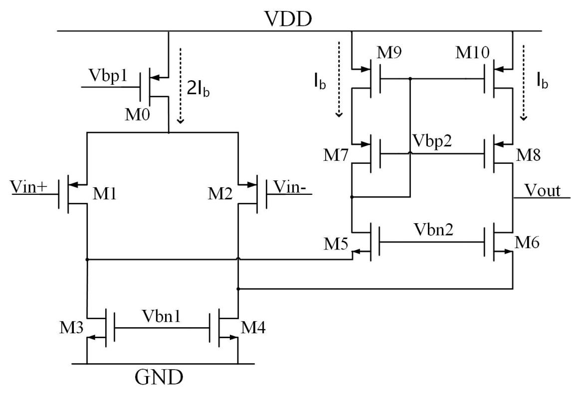
Figure 1: The conventional folded cascode amplifier
Folded cascode structure is a good design scheme, as shown in Figure 1. The input is a differential input of two PMOS transistors, and PMOS is used as the input because compared to NMOS, PMOS has lower flicker noise and non-dominant poles [8]. This structure has the advantages of high input impedance, low output impedance, high gain and wide bandwidth, and reduced power consumption compared to two-stage operational amplifiers. The bias current given to M0 is 2Ib, and the current flowing through M5 and M6 is Ib, so M3 and M4 bear the role of high current 2Ib. However, these two transistors only act as current sources and are limited to providing a folded node for the drain terminals of M1 and M2, which cannot fully play their role [9].
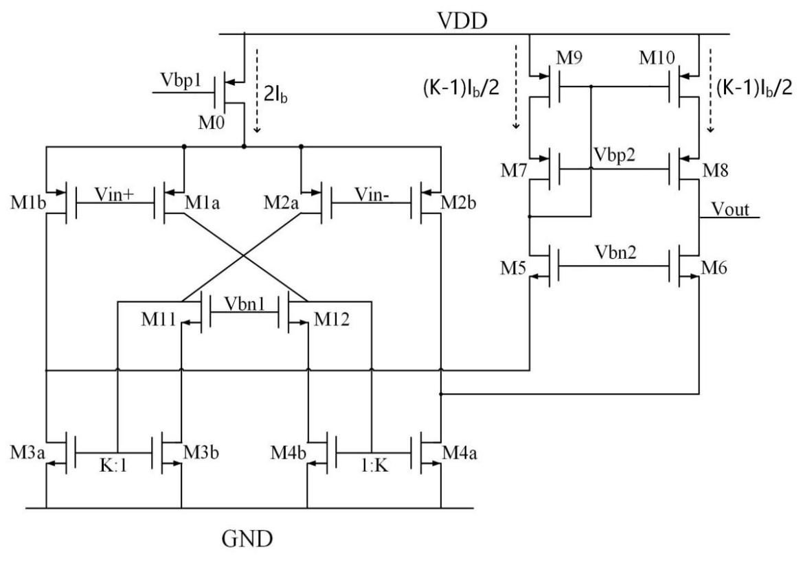
Figure 2: The recycling folded cascode amplifier
On the basis of FC structure, retaining the structure on the right and modifying the structure on the left, a recycling folded cascode amplifier was designed, as shown in Figure 2. This structure mainly splits the original folded current source transistors M3 and M4 into two transistors, forming a structure of two current mirrors with a proportional size of K. In order to match the current mirror, the two input transistors are also divided into two equally sized transistors, and the current flowing through each transistor is Ib/2. By applying a bias voltage to M11 and M12, the differential current is input and transmitted to M3b and M4b through M11 and M12. The current is multiplied by K times by the current mirror and transmitted to the output load. The K value here is generally selected as 3, so the current of the folded structure is smaller than that of the folded structure in FC. In terms of size, the dimensions of M11 and M12 should be kept similar to those of M5 and M6 to ensure consistent drain potentials in M3a, M3b,andM4a, M4b, in order to improve the matching degree of the current mirror [9].
2.2. Analysis of small signal circuits
2.2.1. Low frequency gain
The transconductance and output resistance of the conventional folded cascode amplifier are
\( {G_{mFC}}={g_{m1}} \) (1)
\( {R_{oFC}}={g_{m6}}{r_{o6}}({r_{o2}} \) || \( {r_{o4}} \) )|| \( {g_{m8}}{r_{o8}}{r_{o10}} \) (2)
The transconductance and output resistance of the recycling folded cascode amplifier are, respectively
\( {G_{mFC}}={g_{m1a}}(1+K) \) (3)
\( {R_{oFC}}={g_{m6}}{r_{o6}}({r_{o2b}} \) || \( {r_{o4a}} \) )|| \( {g_{m8}}{r_{o8}}{r_{o10}} \) (4)
Then the gains of both are
\( {{A_{V=}}G_{m}}{R_{o}} \) (5)
Compared to traditional FC operational amplifiers, the input transistor of RFC is divided into four transistors of the same size, and the size is half of the original, reducing W to half of its original size. The transconductance of a single transistor is reduced to half of its original value, and due to the multiplication of the current mirror (usually with a K value of 3), the transconductance is doubled. With the same output impedance, the gain is 2 times higher than before.
The output impedance of RFC has also increased compared to FC, due to the reduction in size resulting in a decrease in the current passing through, thereby increasing the on resistance. Although this is not conducive to the matching of subsequent circuits, it can increase the gain of this stage by 8-10 dB compared to the original.
High gain can also increase PSRR. With the same power injection, the loop gain of RFC is higher, improving the performance of PSRR.
2.2.2. Gain bandwidth basis
The bandwidth of the conventional folded cascode amplifier is
\( {GBW_{FC}}=\frac{{G_{mFC}}}{2π{C_{L}}} \) (6)
The bandwidth of the recycling folded cascode amplifier is
\( {GBW_{RFC}}=\frac{{G_{mRFC}}}{2π{C_{L}}} \) (7)
As mentioned in the above article, the overall transconductance of RFC is twice that of FC (K=3), so the bandwidth is also twice that of FC. As a result, the wide bandwidth also doubles the response speed of the circuit and is beneficial for suppressing power supply noise. The performance of PSRR is brought to a higher frequency range [10].
2.2.3. Phase margin
Phase margin is the best test to reflect the stability of a circuit. Generally, a circuit can only be considered relatively stable if its phase is greater than 60 ° at 0dB. And the phase margin is also related to the zero and pole points. Compared to the FC structure, RFC has three poles. The main pole is generated by the load capacitance and resistance, while the first non main pole is generated by the parasitic resistance and capacitance at the M6 or M8 source. The second non dominant pole is generated by the parasitic resistance and capacitance at the intermediate node of the current mirror (M3a and M3b or M4a and M4b) [10]. Noticeably, there will also be a zero point generated here, which is a pair of zero pole pairs with the second non dominant pole, but they are both located at a very high frequency and do not contribute significantly to the phase.
The choice of K value also has a certain impact on phase margin. Through simulation, it can be known that both excessively large and small K values will cause a decrease in phase margin. Although the bandwidth becomes wider, the circuit is unstable. So the K value is generally selected between 2-4.
2.3. Big signal analysis
Slew rate
The slew rate refers to the operational amplifier conversion rate of the output voltage, which reflects the adaptability of the operational amplifier to the speed of signal changes. It is an important parameter for measuring the operating speed of the operational amplifier under the action of large signals. Assuming an increase in Vin+, M1a and M1b will turn off, causing M4a and M4b to also turn off. The source potential of M6 will increase, and the channel at the source will be pinched off from a physical perspective,causing M6 to also turn off. Due to the increase in the drain potential of M2b, it enters the deep linear region. The current of 2Ib flows through M2a and is amplified K times by the current mirrors of M3a and M3b, and then enters the load capacitor 1:1 through the M9 and M10 current mirrors. So the RFC structure slew rate can be expressed as
\( {SR_{RFC}}=\frac{2K{I_{b}}}{{C_{L}}} \) (8)
The slew rate of FC structure can also refer to the analysis of RFC, but with the missing multiplication of the current mirror in the middle, it can be expressed as
\( {SR_{FC}}=\frac{2{I_{b}}}{{C_{L}}} \) (9)
Comparing the two, it can be seen that under the same power consumption, the slew rate of RFC is K times that of FC. However, in reality, it cannot reach K times because even if the transistor is completely turned off, there will still be some effect that causes current to flow. Choosing the appropriate size can also increase the multiplier as much as possible.
3. Simulation results
This article simulates FC and RFC structures using Cadence's CMOS 0.18 μm process, mainly to simulate and verify the parameters mentioned in this article. Both have a bias of 15 μA, a power supply voltage of 3.3V, and a load capacitance of 10pF. Table1 shows the result of the simulation.
Table 1: Amplifier characterization results
PARAMETER | FC | RFC |
Low frequency gain [dB] | 57.40 | 63.33 |
GBW [MHz] | 196.7 | 371.76 |
Bias current [μA] | 15 | 15 |
Capacitive load [pF] | 10 | 10 |
Slew rate(average) [V/μs] | 251.5 | 377.5 |
5% Settling time [ns] | 9.0 | 4.5 |
Phase margin [deg] | 82.22 | 74.53 |
CMRR [dB] | 79.92 | 88.57 |
|PSRR| [dB] | 5.35 | 0.67 |
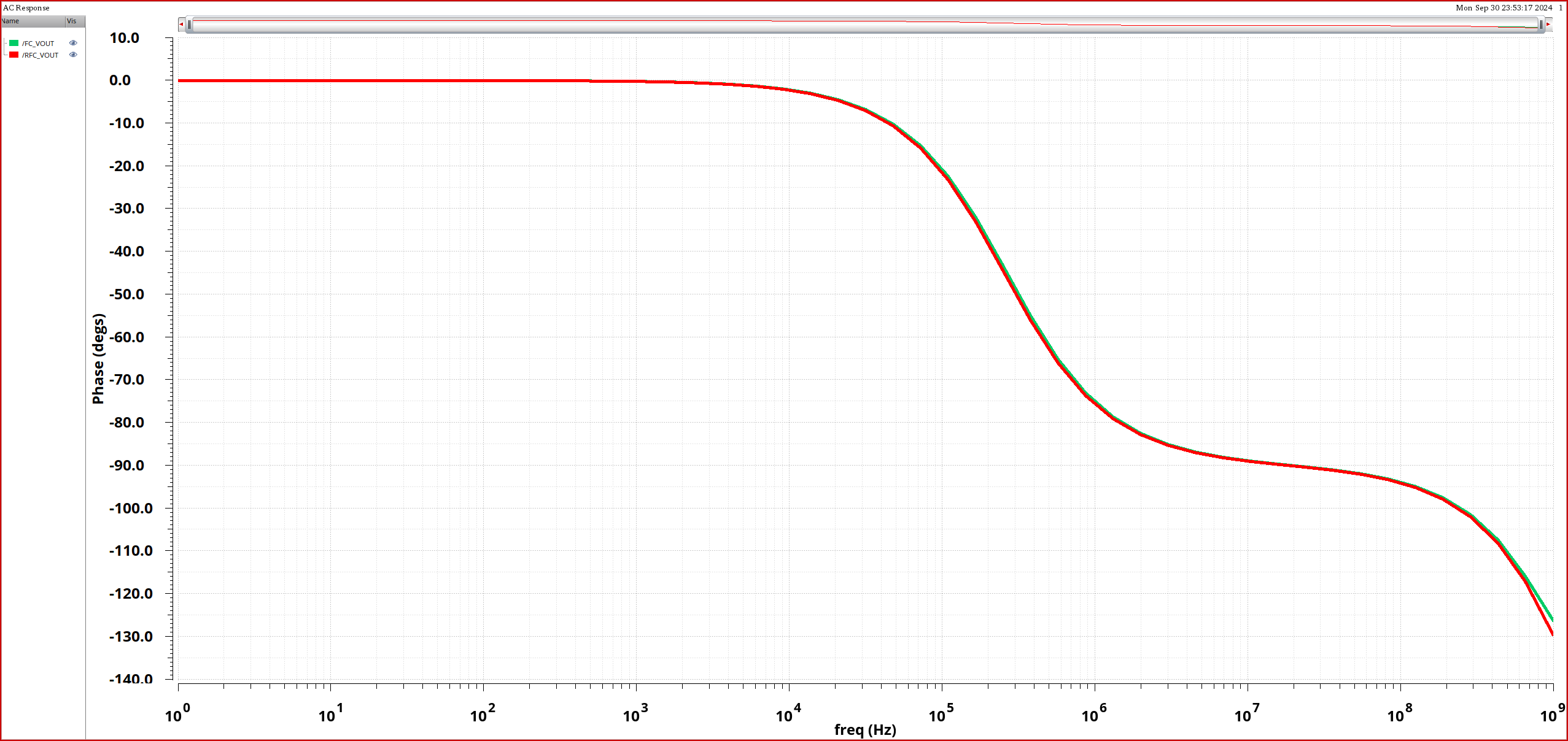
The K value selected in this article is 3, and the input transistor size of the FC structure is twice that of RFC, while the rest remains unchanged. The low-frequency gain of the FC structure is 57.40dB, while the gain of the RFC structure is 63.33dB, with a difference of 6dB. Figure 3 (a) shows the AC simulation, where the operational amplifier both provide a DC voltage of 1.5V and an AC voltage of 1V. The red line represents the output of RFC, and the green line represents the output of FC. Under the same load, the gain bandwidth of RFC is roughly 1.89 times that of FC, possibly due to the influence of some parasitic capacitance. Figure 3 (b) shows the phase situation, and it can be observed that the two curves almost overlap.
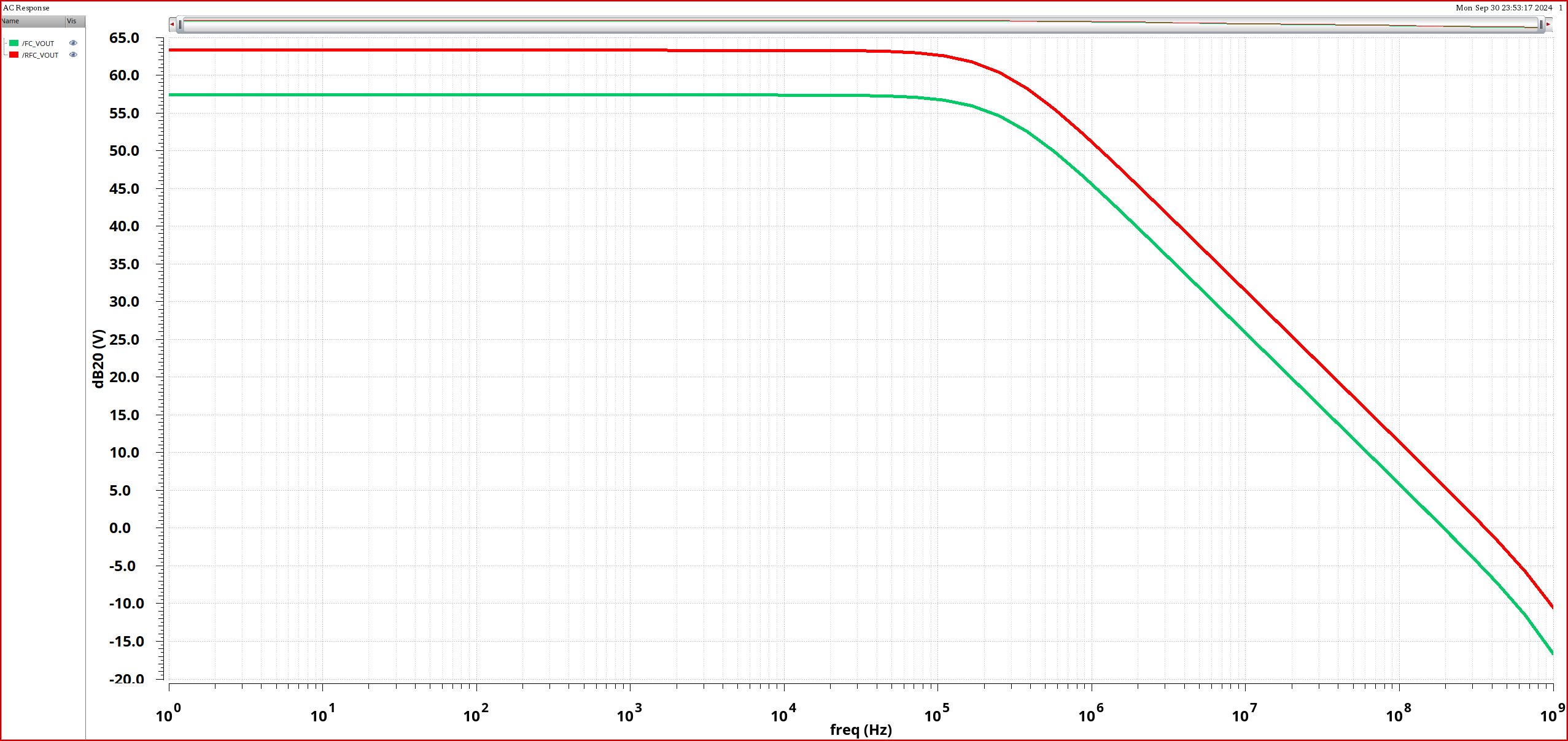
(a)
(b)
Figure 3: Amplifiers AC response. (a) Magnitude. (b) Phase
The slew rate of the large signal is only 1.5 times, indicating that there is still a large turn off current generated in this process, as shown in Figure 4. Both types of operational amplifiers are connected in the form of source followers, with the purple line as the input current, set as a square wave with an amplitude of 900mV, a period of 1ms, a rise time and a fall time of 1ns, and a duty cycle of 50%. The phase margin of both circuits is above 60 °, suggesting that both circuits are in a relatively stable state. However, due to the higher complexity of RFC circuits compared to FC, the phase margin may decrease.
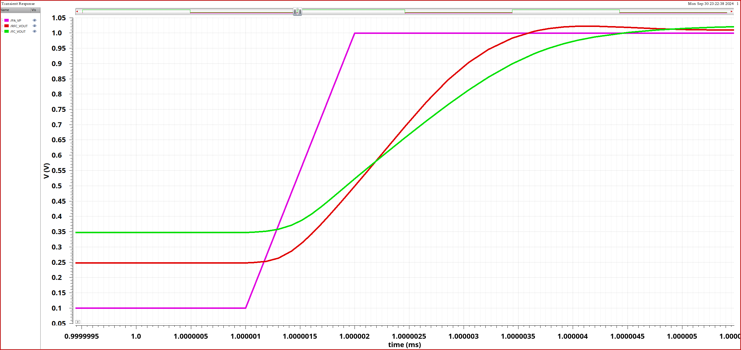
Figure 4: Amplifier large signal step response
The common mode rejection ratio is within the normal range for both, which can effectively suppress common mode input. The power suppression ratio of RFC is higher than that of FC. A higher PSRR means that the noise amplitude in the power output is relatively small, while a lower PSRR indicates greater noise interference. Therefore, the larger the PSRR, the stronger the device or system's ability to suppress power supply noise.
4. Summary
This article requires the design of a high-efficiency operational transconductance amplifier. Based on the folded cascode amplifier, a recycling folded cascode amplifier is designed. The improvement is to turn the folded current source into a current mirror and match it with other transistors. This increases the gain and bandwidth at low frequency while maintaining the same power consumption, but slightly reduces the phase margin. Two circuits were simulated and verified using CMOS technology at Cadence 0.18 μm, and a bias circuit was provided to increase gain by 6dB and bandwidth by 1.89 times; Sacrificing a certain level of complexity resulted in improved performance in other aspects as well. The power supply voltage provided in this article is 3.3V, and the power consumption of both circuit structures is 49.5 μW so they can be applied to portable mobile communication devices with low power consumption and high efficiency.
The design of this article inevitably has certain shortcomings, such as no simulating noise and no drawing a layout for post simulation verification. Further in-depth research will be conducted in the future. Secondly, in large signal simulation, when the operational amplifier is connected in the form of a source follower, both structures of circuits have not implemented rail to rail. If the output does not reach the rail, it will result in higher distortion and noise, affecting the overall signal integrity of the system. Therefore, a high-efficiency rail to rail operational amplifier will be further designed.