

1. Introduction
As a semiconductor material, silicon has stable chemical properties, good conductivity and insulation properties, and a wide temperature range. These characteristics make silicon an ideal choice for manufacturing integrated circuits. It not only provides stable substrate materials required for manufacturing electronic devices, but also has adjustable electronic characteristics, enabling integrated circuits to achieve complex functions and high performance.
But with the development of science and technology, scientists have discovered many new materials that have obvious advantages in electron mobility, photoelectric properties, and heterostructure manufacturing. So does this mean that silicon can withdraw from the historical stage of integrated circuits and be completely replaced by new materials? To address these concerns, we will explore three alternative materials for silicon in the following content and analyze their feasibility in integrated circuits from different perspectives.
2. Carbon Nanotubes
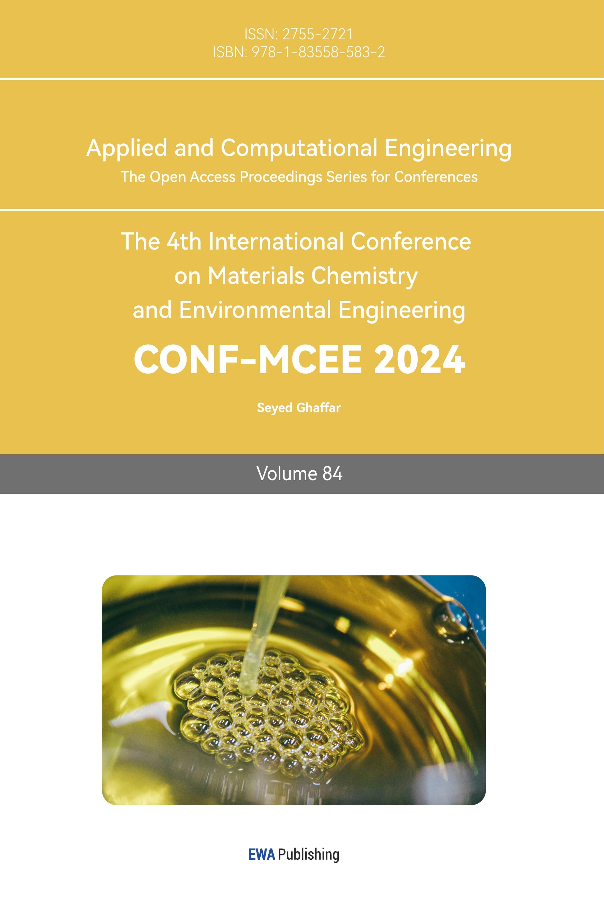
Carbon nanotubes are one-dimensional quantum materials with a unique structure, featuring nanoscale radial dimensions and micrometer-scale axial dimensions. The ends of the tubes are typically closed. Carbon nanotubes consist of coaxial circular tubes composed of several to dozens of layers of carbon atoms arranged in a hexagonal shape. The interlayer distance is approximately 0.34 nm, and the diameter generally ranges from 2 to 20 nm.
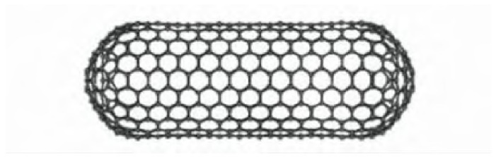
Figure 1. Schematic of SWNT
Since its first discovery by Japanese electron microscopy expert Lijima [1] in 1991 during the preparation process of C60 using arc method, carbon nanotubes have exhibited broad application prospects due to their unique structure and excellent mechanical, electrical, and chemical properties [2]. As a result, they have attracted tremendous attention from scientists in fields such as materials, physics, electronics, and chemistry, and have become a research frontier and hotspot in the international field of new materials. Carbon nanotubes can be divided into single-walled carbon nanotubes (SWCNT) and multi-walled carbon nanotubes (MWCNT) depending on the number of layers inside the tube. After more than 20 years of in-depth research by scientists from various countries, it has been found that carbon nanotubes have the following characteristics:
The diameter of carbon nanotubes can be regulated in the range of several nanometers to tens of nanometers, and the length can range from a few micrometers to several centimeters. At the same time, they can be single walled or multi walled structures, consisting of multiple concentric tube walls inside. Carbon nanotubes are approximately 100 million times longer than their diameter, which is considered very small in our everyday experience, but larger than any other known cylindrical nanostructure. This makes carbon nanotubes a valuable tool for designing small objects, such as processor chips [3].
Figure 2. Cross section of carbon nanotubes
Carbon nanotubes have high strength and stiffness, stronger and lighter than traditional materials such as steel and aluminum. This makes carbon nanotubes have important applications in the reinforcement and strengthening of nanomaterials, such as in the manufacturing of strong and tough composite materials and high-performance fibers.
Carbon nanotubes are excellent electronic conductors with high electron mobility and low resistivity. This makes carbon nanotubes have broad application prospects in electronics and nanoelectronic devices, such as transistors, sensors, and transparent conductive films.
Carbon nanotubes have excellent thermal conductivity and can efficiently conduct heat. This makes carbon nanotubes have potential applications in the fields of thermal management and heat dissipation, such as for manufacturing thermal interface materials and thermal conductivity tubes.
Carbon nanotubes also have unique optical properties, and their optical absorption and fluorescence properties are related to their diameter and structure. This makes carbon nanotubes have broad application prospects in fields such as optoelectronics, optical sensing, and biomedicine.
In summary, the various characteristics of carbon nanotubes determine their excellent application in the field of chip processors. In theory, processors made from carbon nanotubes can be even smaller than current transistor technology. Just like today’s processors, smaller size means less energy consumption. For mobile devices, this translates to less heat and longer battery life. In addition, the electrical properties of carbon nanotubes enable faster switching on and off than silicon transistors, allowing for faster operation speeds than current chips. However, contrary to popular belief, carbon nanotube processors may not necessarily be more environmentally friendly than traditional silicon-based processors in terms of their manufacturing processes and potential biodegradability. Furthermore, the production of carbon nanotube processors can be challenging and expensive, much like the latest high-end processors for luxury devices.
3. Gallium Arsenide
Gallium arsenide is an inorganic compound, a black gray solid with a melting point of 1238 ℃. It can stably exist in the air below 600 ℃ and is not corroded by non oxidizing acids.
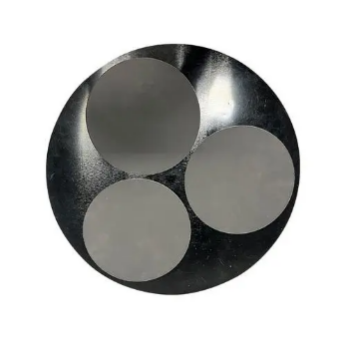
Figure 3. Epi-Ready GaAs Wafer
Gallium arsenide is an important semiconductor material, known as the “semiconductor nobility” due to its high price as a second-generation semiconductor. Gallium arsenide is internationally acknowledged as the most advanced compound semiconductor material after silicon, possessing superior characteristics such as high frequency, high electron mobility, high output power, low noise, and good linearity. As such, it is one of the most crucial supporting materials for optoelectronic and microelectronic industries. When compared to traditional semiconductor materials such as silicon and germanium, gallium arsenide has numerous advantages.
Gallium arsenide has some better electronic properties than silicon, such as higher saturation electron velocity and electron mobility, allowing gallium arsenide to be used in applications above 250 GHz. If equivalent GaAs and Si devices both operate at high frequencies, GaAs will have less noise. Also because gallium arsenide has a higher breakdown voltage, gallium arsenide is more suitable for operating in high-power situations than the same Si device. Due to these attributes, gallium arsenide circuits find applications in mobile phones, satellite communications, microwave point-to-point connections, and radar systems. etc. Gallium arsenide was used to make Gunn diodes to emit microwaves. Although today’s RFCMOS made of silicon as the base material can achieve high operating frequencies and high integration, it has inherent physical shortcomings such as low breakdown voltage, easy substrate loss in high-frequency environments, and poor signal isolation. Low output power density makes it difficult to compete with gallium arsenide in power amplifier and radio frequency switch applications.
Another benefit of gallium arsenide is that it is a direct energy gap material, making it suitable for use in light-emitting devices. In contrast, silicon is an indirect energy gap material, and the light it produces is comparatively weak. Recent technology can use silicon to make LEDs and apply them in the laser field, but the luminous efficiency is still not ideal.
Gallium arsenide is considered an ideal material for semiconductors because of its fast switching speed. In the 1980s, it was generally believed that the main material in the microelectronics market would change from silicon to gallium arsenide. The first companies to try to switch materials were supercomputer suppliers Cray Corporation, Convex Computer Company and Alliant Computer Systems. These companies They are all trying to seize the leadership position in CMOS microprocessor technology. Cray finally built a gallium arsenide-based machine called the Cray-3 in the early 1990s. However, this achievement had not yet been fully utilized. The company went bankrupt in 1995 and was acquired by Silicon Valley Graphics in 1996. After various difficulties, the original name was resurrected after 2000. In addition, Gallium arsenide is less susceptible to interference from natural radiation than silicon and is less prone to false signals [4].
Gallium arsenide material also has characteristics such as heat resistance, radiation resistance, and sensitivity to magnetic fields. Therefore, devices manufactured with this material also have special applications and diversity, and their applications have extended to fields that cannot be achieved by silicon and germanium devices. Entering the 5G era, the second generation semiconductor represented by gallium arsenide is widely used in the manufacturing of integrated circuits such as high-frequency, high-speed, high-power, low noise, high-temperature resistance, and radiation resistance [5]. It has developed into a key technology for modern electronic information products and the “information highway”. Gallium arsenide is also an indispensable component for high-frequency communication in optoelectronics and mobile phone networks. In recent years, with the surge in the Internet of Things, the Internet of Vehicles, and Al applications, countries have accelerated the construction of 5G infrastructure. In addition, the introduction of facial recognition function in Apple’s iPhone X has driven a significant increase in demand for gallium arsenide VCSEL and higher-order communication components.
Of course, gallium arsenide materials also have some unfavorable factors, such as high melting point vapor pressure, difficult to control composition, slow single crystal growth rate, weak mechanical strength, poor integrity, and expensive prices, which greatly affect their application level. Especially in terms of human health, on October 27, 2017, the International Agency for Research on Cancer (IARC), which is the specialized cancer agency of the World Health Organization (WHO), released a preliminary list of carcinogens. Arsenic and inorganic arsenic compounds were included in the Class 1 carcinogen list, which signifies that they are known to be carcinogenic to humans.” However, the toxicity of gallium arsenide has not yet been fully studied. Because it contains arsenic, research has shown that arsenic is toxic and a carcinogen. However, because the crystals of gallium arsenide are very stable, if the body absorbs a small amount, it can actually be ignored (referring to “short time”, but it will still accumulate into biological toxicity over a long time, requiring irregular physical examinations). When the wafer polishing process is performed (the wafer makes the surface particles smaller), the surface area will react with water, releasing or decomposing a small amount of arsenic. This point has recently been made when looking at environmental, health and safety aspects of gallium arsenide (like trimethylgallium and arsenic), as well as studies on industrial hygiene monitoring of organometallic precursors. So, workers should avoid direct contact with arsenic containing substances through the skin, and protective equipment must be used effectively. Arsenic waste should be properly handled, and workers should receive training in hazard identification, awareness, and prevention, The occurrence of arsenic exposure among workers can only be prevented through personal protection and management and prevention of the working environment.
4. Silicon Carbide
Silicon carbide is a compound semiconductor material composed of silicon and carbon. Its bonding force is very strong, and it is very stable in thermal, chemical, and mechanical aspects. There are various polytypes (polycrystalline forms) in SiC, and their physical property values vary. 4H-SiC is most suitable for power components. Silicon carbide is an inorganic compound that appears as a colorless crystal but exhibits a bluish-black color when impurities are present. It has a melting point of approximately 2700°C and shows strong resistance to oxidation at high temperatures.
Since the successful laboratory preparation of silicon carbide single crystals by the Lely method at the Philips Research Laboratory in 1955, over the past 60 years, research institutions and companies in developed countries and regions such as the United States, Europe, and Japan have continuously innovated and improved the preparation techniques and equipment for silicon carbide single crystals. This has given rise to a significant advantage in the field of silicon carbide single crystal and chip technology and industrialization.
The wide bandgap of SiC allows for higher operating temperatures, enabling efficient power conversion and reducing thermal management requirements. Its high breakdown electric field enables the design of compact and robust power devices capable of handling high voltages. The high thermal conductivity ensures effective heat dissipation, improving device reliability and allowing for higher power densities. Additionally, the high electron saturation velocity enables faster switching speeds, making SiC ideal for high-frequency applications. Furthermore, SiC’s radiation-resistant properties make it suitable for use in space and other high-radiation environments. Overall, these unique physical properties of SiC make it a promising material for a wide range of demanding applications. thereby reducing energy consumption and decreasing the size of end products. Silicon carbide has a wide bandgap of approximately 3.2 eV, compared to silicon’s narrower bandgap of 1.12 eV, which is roughly one-third of silicon carbide’s bandgap. This suggests that silicon carbide significantly outperforms silicon in terms of high-voltage tolerance. Additionally, silicon carbide exhibits a significantly higher thermal conductivity than other materials, allowing silicon carbide devices to operate at higher temperatures. Its operational temperature can reach up to 600°C, while silicon devices are limited to around 300°C. The wider bandgap ensures that silicon carbide can withstand higher electric field strengths, making it ideal for the production of high-voltage, high-frequency power devices, which play a crucial role in emerging sectors such as electric vehicles, 5G base stations, satellites, and other industries.
However, silicon carbide materials also have some drawbacks, primarily related to production difficulty and cost control. The single crystal growth rate of silicon carbide is extremely slow, at only 0.1-0.2 mm per hour, in contrast to single crystal silicon’s growth rate of 1-10 mm per hour, with silicon being capable of growing a crystal of about 2 meters in 72 hours. On the other hand, silicon carbide grows a crystal of only 2-3 centimeters in 144 hours, which is less than one percent of silicon’s growth rate. Silicon carbide wafers are mainly available in 6-inch and 8-inch sizes, while silicon wafers can reach up to 12 inches. Another major factor affecting the cost of silicon carbide is its high hardness; it has a Mohs hardness of 9.5, sharing a structure with diamond. This means it lacks ductility, is rigid, and easily fractures. Cutting, grinding, and polishing processes in the production of silicon carbide often result in crystal fractures, making lithography and cutting processes exceedingly difficult and leading to significant losses. Cutting 35-40 pieces from a 3 cm thick ingot of silicon carbide takes 120 hours, far slower than cutting silicon ingots, and this increases the cost. Furthermore, silicon carbide possesses over 200 different homo-polytypic crystal structures, which impose high demands on environmental temperature and other control conditions during the crystal growth process. The preparation process requires higher temperatures and more energy to complete. Silicon sublimates at around 1400 degrees, while silicon carbide wafers require approximately 2000 degrees for crystal growth, leading to greater demands on furnace equipment. Moreover, the long growth cycle of silicon carbide results in thinner ingots, increasing the difficulty of yield control.
Silicon carbide, as a typical representative of third-generation semiconductor materials, gallium nitride (GaN) is also one of the most mature and widely used wide bandgap semiconductor materials in crystal production technology and device manufacturing. It has given rise to a global industry chain covering materials, devices, and applications. In the foreseeable future, new energy vehicles will be the main application scenario of silicon carbide power devices. As a technology pioneer, Tesla has taken the lead in integrating all-silicon carbide modules into Model 3, and other first-tier car companies are also planning to expand the application of silicon carbide. As the manufacturing cost of silicon carbide devices decreases and process technology gradually matures, the future of the silicon carbide power device industry is promising.
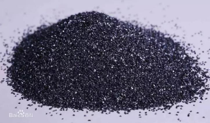
Figure 4. Schematic of HTCVD
5. Conclusion
The unique characteristics of second and third-generation semiconductors enable them to demonstrate outstanding performance in multiple commercial sectors and have a significant impact on improving energy efficiency, reducing carbon emissions, and driving technological innovation. As technology continues to advance, the application areas of silicon carbide semiconductors will continue to expand, and further cost reductions will provide more opportunities for future semiconductor technology development.